TECHNOLOGY
Semiconductor Inspection Solutions
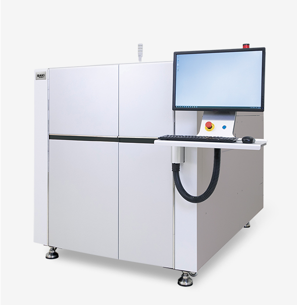
SAKI develops state-of-the-art automated optical and X-ray inspection systems for advanced semiconductor packaging processes.
Our solutions accurately detect defects in microbumps, TSVs, TGVs, and other critical structures. We address the challenges of increasingly miniaturized and complex semiconductor device manufacturing, supporting high-reliability quality assurance in the era of AI, 5G, and electric mobility.
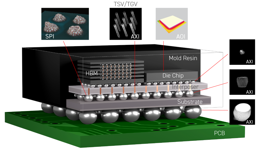
Inspection Targets in Semiconductor Packaging
01
3D Microbump Inspection
SAKI’s high-resolution 3µm SPI system delivers precise, automated inspection of finely printed microbumps. Despite being an automated visual inspection solution, it achieves measurement accuracy comparable to 3D metrology equipment. It also supports solder paste inspection for stencils with apertures of 50µm or less.
02
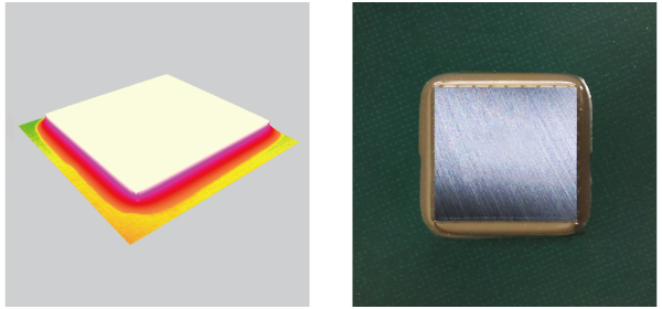
Die Surface Height Measurement
SAKI’s advanced 3µm resolution AOI system measures die surface height with exceptional accuracy, enabling the detection of chips and foreign matter beneath mirror-like surfaces. Saki’s proprietary imaging technology ensures highly accurate height measurement even on highly reflective surfaces – traditionally challenging for optical inspection.
Die Chip Detection Using 3 µm AOI
03
Simultaneous X-ray Inspection of Microbumps, C4 Bumps, and BGA Bumps
High-Resolution X-Ray Insprection
SAKI’s high-resolution AXI solution provides automated X-ray inspection of internal solder joints in semiconductors. To inspect the microbumps between the semiconductor chip and the interposer, we have achieved high-resolution tomographic imaging and a large depth of field through the rigidity and precision of the stages that comprise the planar CT. Meticulous system calibration further guarantees stable and precise inspection results.
“One Scan, Multi-Layer Inspection”
A key feature of SAKI’s AXI system is its ability to accurately distinguish and inspect multiple solder layers in a single scan, even for complex multi-layer semiconductor package structures. Unlike conventional systems that require multiple passes, SAKI’s proprietary planar computed tomography (PCT) technology enables complete full-layer inspection and analysis of all solder joints within a chip with just one scan. This reduces inspection time and significantly minimizes X-ray exposure.
Multilayer Package Inspection
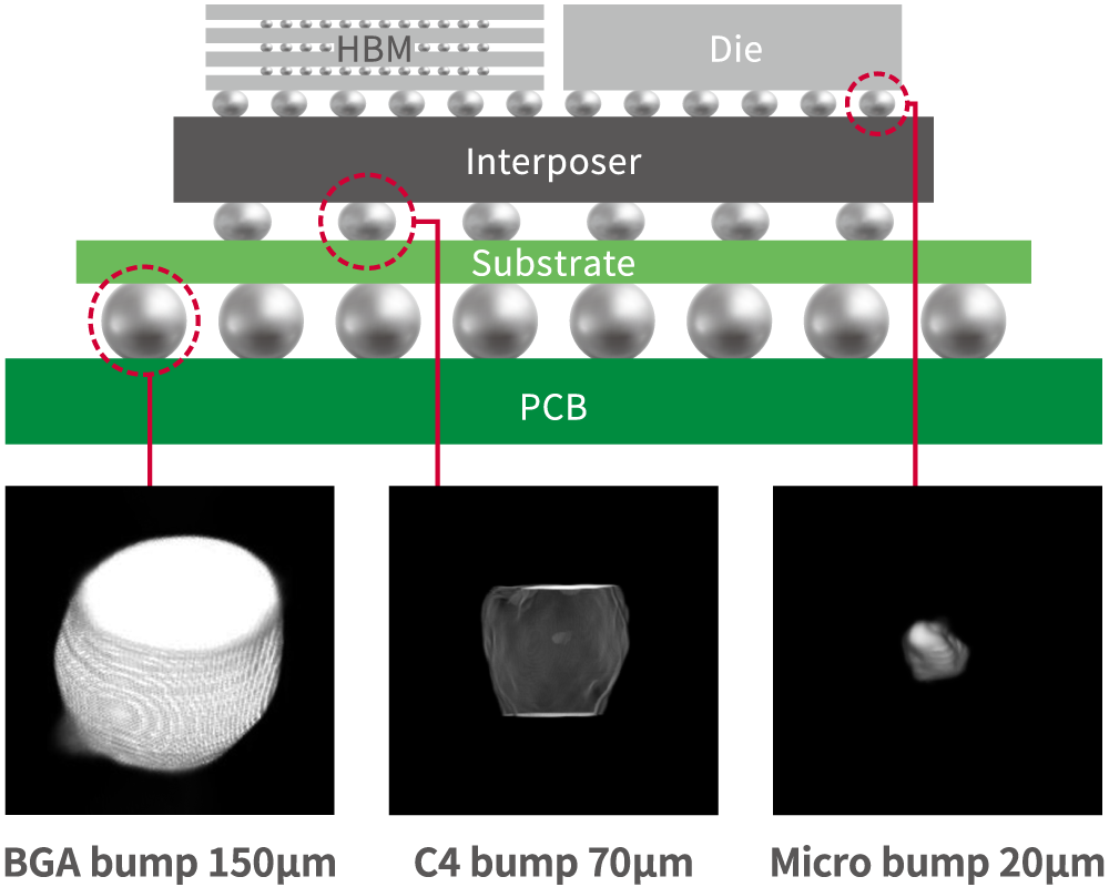
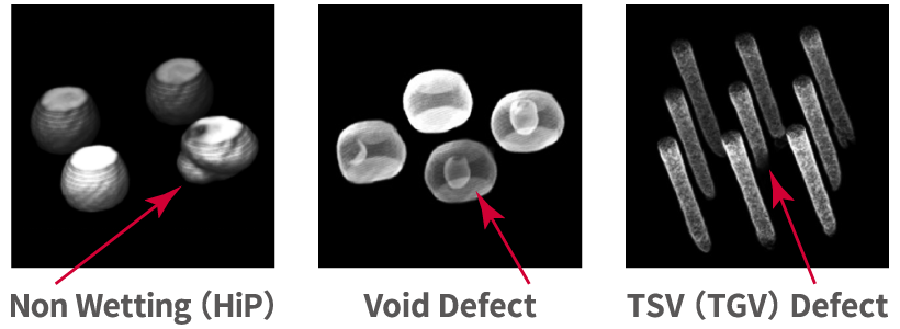
SAKI’s 3D CT inspection delivers exceptional high-resolution imaging for complex semiconductor packages. It excels in handling challenging insprections such as microbump (20µm) bridge insprection, C4 bump (70µm) and BGA bump (150µm) non-wetting and void insprection – ensuring thorough evaluation and analysis of internal structures.
High-Speed Inspection for In-Line Implementation
SAKI’s AXI solutions are optimized for in-line operation, meeting the cycle time demands of SMT production processes. Through propriatary advanced high-speed processing, SAKI’s AXI synchronizes image acquisition with data processing to achieve real-time 3D data capture and inspection. Saki is committed to evolving semiconductor inspection to meet future industry challenges.
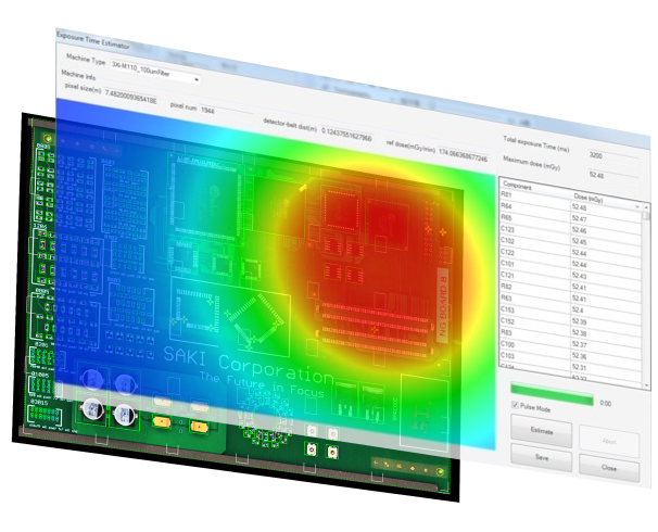
Minimizing Radiation Exposure Risk
To support both product quality and operator safety, SAKI’s AXI systems are equipped with a radiation dose simulator. This allows for predictive dose control and adaptive imaging optimization. Additionally, X-rays are emitted only during image capture, further reducing overall radiation exposure.
X-ray Dosage Simulator
SAKI’s X-ray Inspection Technology >
SAKI’s 3D X-ray Inspection Machine for IGBT Power Modules >
SAKI remains committed to driving innovation in semiconductor inspection. Looking ahead, we will expand our portfolio to include wafer-level inspection solutions, reinforcing our commitment to end-to-end quality assurance throughout the semiconductor manufacturing process.
Related Solutions
3D-SPI
3D Solder Paste
Inspection Machine
3D-AOI
3D Automated Optical Inspection Systems
3D-CT AXI
Inline 3D-CT Automated
X-ray Inspection Systems