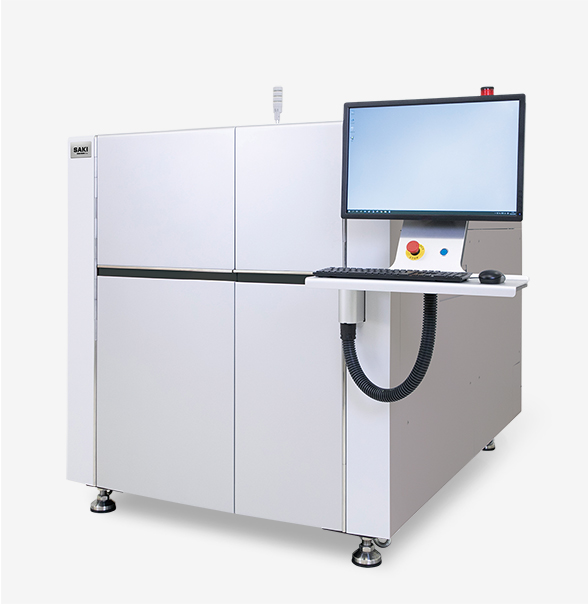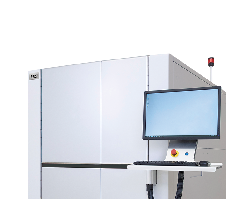
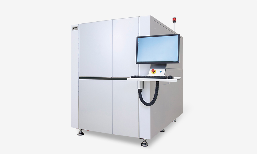
Inline 3D X-ray Inspection Machine for IGBT Power Modules
Power
Module AXI
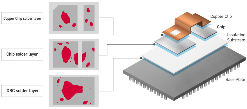
A 3D-CT X-ray inspection system that is ideal for Power module inspection with multi-layered solder, the 3D-AXI achieves the industry’s fastest speed inspection while reliably detecting difficult defects such as voids in three-layer soldering.
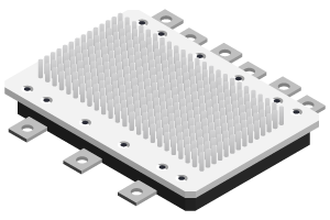
Power module with multi-layered solder that SAKI can inspect
01

Unrivaled Defect Detection Ability with 3D-CT X-Ray Inspection
- Unique Planar CT Technology for High-precision 3D inspection
- Accurate detection of thin voids in difficult-to-inspect multi-layer

Planar CT technology suitable for solder layer separation
In power module, 2D inspection using X-rays from directly above makes it impossible to measure voids because the solder layer overlap with heat dissipation fin and spacer.
With SAKI’s unique Planar CT technology, which specializes in imaging flat objects, each solder layer is separated to accurately detect voids.
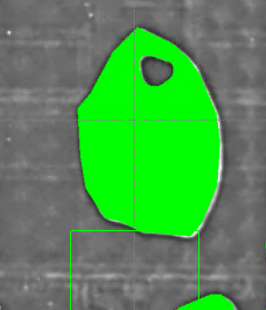
Cross-sectional image of IGBT power module
SAKI’s high-precision hardware design is essential for the creation of high-definition 3D data. The ultra-rigid gantry and high-resolution linear scale provide incredible accuracy in positioning for stable imaging.
Gantry position information is reflected in real-time calculations to obtain high-definition 3D images with clear edges.
Supports inspection of Heavy thick, multi-layered power module
SAKI’s IGBT power module X-ray inspection system uses a high-power X-ray Tube, making it suitable for inspecting heavy thick power module. It can reliably detect void defects in three-layer soldering without being affected by noise from heat dissipation fin.
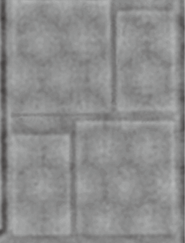
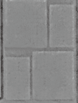
Heat sink shadows are removed
SAKI’s unique image processing technology separates the solder layer from radiation fins and removes the shadow of the radiation fins to erradicate image noise and more accurately detect voids that occur in the solder layer.
Before Noise Cancelation (left) After Noise Cancelation (right)
Highly accurate void inspection
Pass / fail judgments are made by measuring the void area of the solder layer. The noise cancellation filter of the new void inspection algorithm accurately detects thin voids that have been historically problematic for inspection.
Prior to application of the noise cancellation filter, artifacts other than the central void are also detected (left image). After filter application, the shape of the defect is detected more accurately (right image).
Before Noise Cancelation (left) After Noise Cancelation (right)
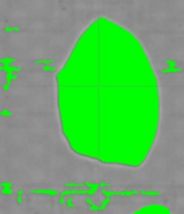
(green areas are recognized as defective)
Supports inspection of Slim and lightweight DSC power module
Recently, advances in DSC technology have led to an increase in the number of slimmer and lighter power modules.
Even with such multi-layer components, SAKI’s 3Xi-M200 can clearly separate layers such as spacers from multiple solder layers and detect void defects.
Cross-sectional view of DSC power modules

Debug without stopping the production line
The offline debugging function enables the collection and debugging of images without stopping the operating equipment. Alongside real-time library updates, a catalogue of historic defect data is saved and can be re-inspected, significantly contributing to overall quality assurance.
02

Industry’s Fastest Inspection Speed
- High-speed inspection achieved through multiple concurrent wide-area imaging processes
- Optimized calculation processing means imaging and calculation processing are completed almost simultaneously
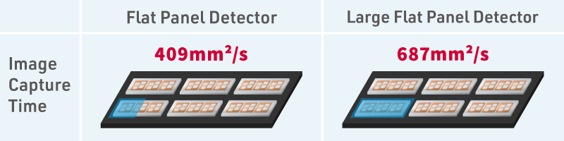
Imaging time reduced with expanded detector field of view
SAKI’s latest technology, all developed in-house, has increased the scan speed by 64%*.
This is achieving imaging speed equivalent to our PCB AXI (M110).
Additionally, the integration of a large, high-sensitivity detector enables the capture of high-quality images in significantly less time.
*Compared to our previous model
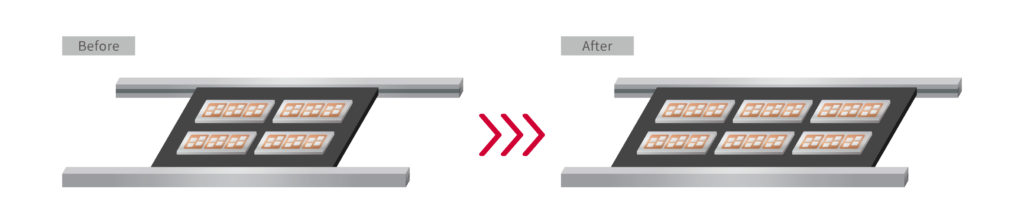
Reducing the cycle time by transporting large jigs
An improved conveyor design allows for the loading of larger carriers, now up to 460mm x 600mm. Through batch imaging and inspection of multiple samples, cycle time is decreased, preparation time is shortened, and operator workload reduced, especially during tray setting.
Imaging process optimization with unique CT calculation technology
SAKI’s combined hardware and software development ensures optimal image processing, with CT calculations presenting almost zero delay to the inspection process.
03

Ease of Maintenance
- Long-life hardware design
- Self-diagnostic function, X-ray dosage simulator and reduction
Long-life hardware design
High-precision, accurate, and stable inspections in a mass production environment require quality, durable hardware.
SAKI’s X-ray inspection machine features a unique ultra-rigid gantry that results in a long equipment lifetime and high repeatability. Designed for the easy replacement of parts, maintenance is greatly improved, while SAKI’s new detector offers significantly reduced component radiation thanks to its redeveloped lead protection design.
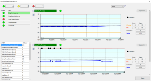
Self-diagnostic functions
Sustaining high-precision, high-accuracy inspection is important to maintain high productivity.
SAKI’s X-ray inspection equipment regularly diagnoses the deterioration of the X-ray source, uneven image brightness, frame distortion, and more. Maintenance can be carried out in a planned manner and high-accuracy can be maintained.
Self-diagnosis prevents sudden equipment failure, reduces equipment downtime, prevents unnecessary replacement of non-defective parts, and reduces maintenance man-hours.
Time Based Maintenance
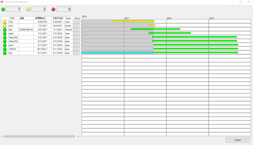
Condition Based Maintenance
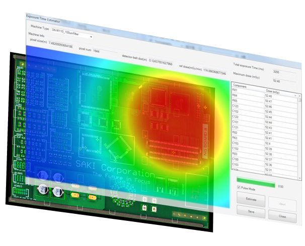
X-ray Dosage Simulator
When performing X-ray inspections, many people are concerned about the risk of component failure due to radiation exposure.
SAKI’s X-ray inspection equipment is equipped with an exposure dose simulator, predicting the exposure dose for each area to optimize imaging conditions. X-rays are irradiated only during imaging, minimizing irradiation.
X-ray dosage simulator
Specification
3Xi-M200
Specification
| Model | 3Xi-M200 |
|---|---|
| Size (W) x (D) x (H)mm (in.) | 1400x2176x1862 (55.12 x 85.67 x 73.31 in) |
| Resolution | 15μm-42μm |
| PCB Clearance | Top : 68mm (2.68 in.) Bottom : 40mm (1.57 in.) |
| Electric Power Requirement | Three Phase 200-240V +/-5%, 50/60Hz |
| X-ray Tube | 180kV, Closed X-ray Tube |
| X-ray Leakage | 0.5μSv/h以下 |
| PCB Size (W) x (L) mm (in.) | 50×460 – 140×440 (1.97 x 18.12 – 5.52 x 17.33 in.) 70×460 – 140×600 (1.97 x 18.12 – 5.52 x 23.63 in.)* |
| Weight | Aprox. 5,200kg |
*Target board size with 2x imaging option
Related Solutions
3D-CT AXI
Inline 3D-CT Automated
X-ray Inspection Systems