Technology
Founded in 1994, SAKI innovated in a crowded and competitive inspection machine market with unique high-speed inspection technology.
Since then, it has continued to grow alongside its customers by sensing new market needs and developing new products.
Introducing the latest technology that supports SAKI’s advanced inspections.
SAKI Technology
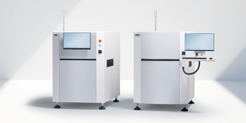
High-speed Inspection Technology
Wide-area imaging to shorten cycle time
Hardware structure that enables high-speed movement of the optical head
Advanced image processing to reduce unnecessary waiting time
3D Image Acquisition Technology
Substrate surface correction technology
Image generation technology
Reduction of library management time
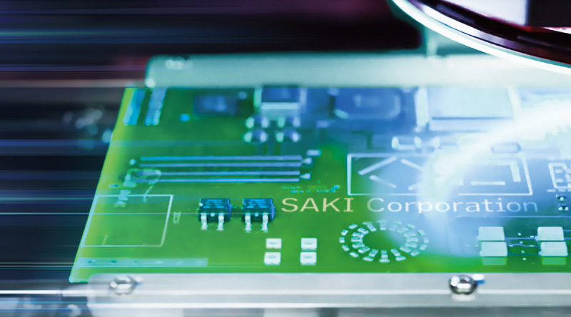
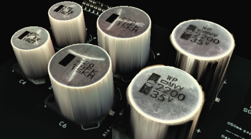
X-ray Inspection Technology
SAKI’s unique Planar CT technology
Image processing technology that increases defect detection ability
High-speed inspection that also supports inline processing
SAKI Solution

AI Inspection Solution
AI Assist : Uses AI to re-assess, reducing operator workload
AI Inspection(AI OCR)
Semiconductor Inspection Solutions
3D Microbump Inspection
Die Surface Height Measurement
Simultaneous X-ray Inspection of Microbumps, C4 Bumps, and BGA Bumps
SAKI’s Design philosophy – Upgrade to Excellence –
Modular Structure Customizable to Fit Inspection Needs
Expandable Items Selectable Specific to Inspection Needs
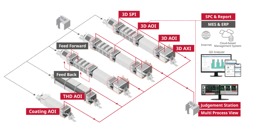
Total Solution
Contributing to reduced costs and labor-saving
Contributing to quality improvement and smart factories