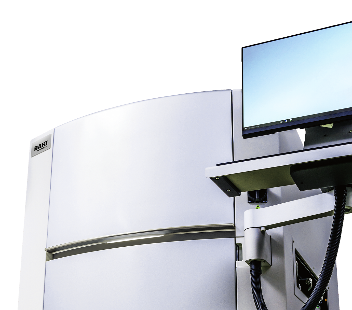
Inline Bottom-Side 2D Automated Optical Inspection Systems
BottomSide-
AOI
A 2D bottom-side inspection machine that automates the final process inspection of printed circuit board mounting, Bottom-Side AOI guarantees the solder quality of through-hole components after the selective, flow and dip soldering process. As board handling and PCB reversal is not required, efficiency is improved.
01

Efficiency
- Equipment design accommodates mounting of large
- Common operations with SMT process

Automatic bottom surface inspection that contributes to investment capital efficiency and labor savings
Prevent damage from manual or automated board handling by eliminating the need to flip the PCBs – Bottom-Side AOI insures quality and productivity by removing the need for manual operation and board reversal.
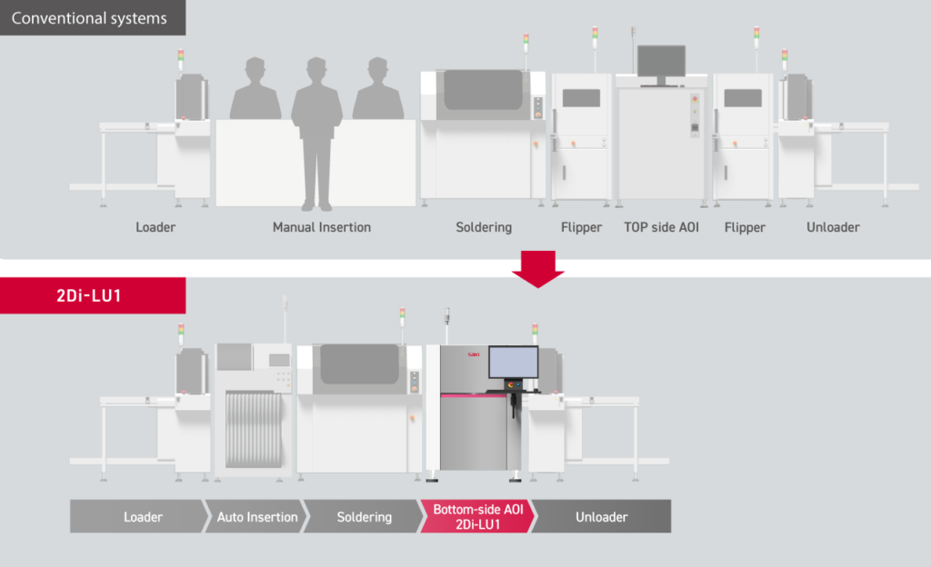
Equipment design that accommodates mounting of large components and heavy boards
The 130mm top clearance and highly rigid conveyor allow the Bottom-Side AOI to accommodate boards with large, odd-shaped through-hole component mounted-PCBs and heavy jigs, greatly expanding the range of inspection processes that can be automated.
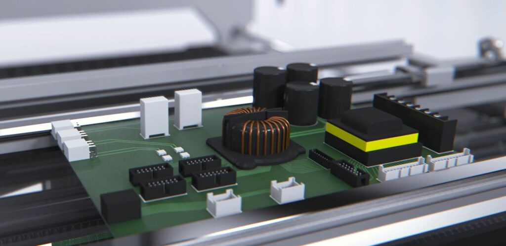
Large, Odd-Shaped Inserted Component Mounted PCBs
Common operations with SMT process
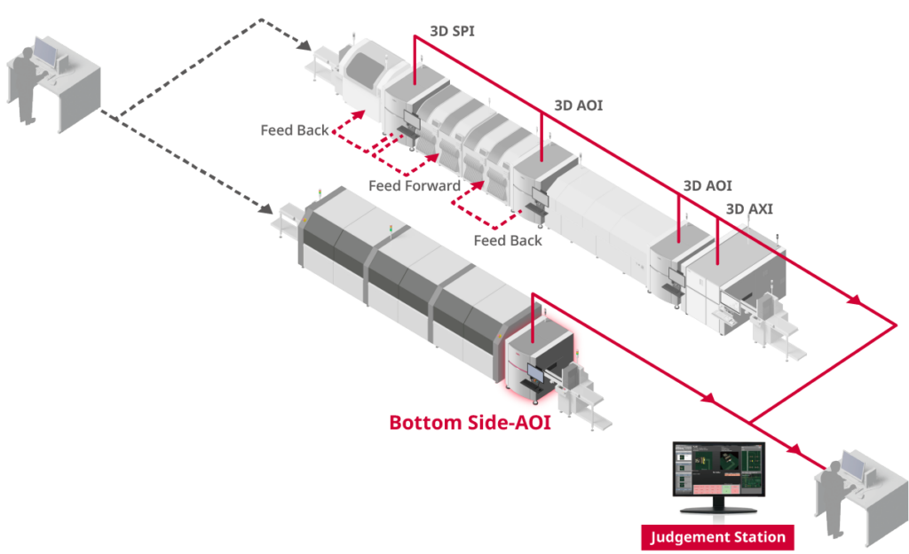
The Bottom-Side AOI uses the same software platform as SAKI’s solder print inspection system (SPI) and post-post reflow inspection system (AOI). Using a common system unifies operations and reduces operator workload.
02

High-speed Inspection
- Rapid inspection with simultaneous full-board imaging
- SAKI’s unique line scan imaging method
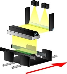
SAKI’s unique line scan imaging method has been applied to 2D bottom-side inspection to achieve consistently high speeds.
High-speed inspection by simultaneous full-board imaging
Through batch imaging using a line sensor camera, images of the entire board are rapidly acquired. Simultaneous full-board imaging means takt time is unaffected by either the number of parts or mounting status.
Hardware designed to provide high-speed, high-accuracy inspection
The simple and stable hardware design of a single-axis drive significantly improves both accuracy and speed. High-speed imaging of a medium size board is undertaken in approximately 10 seconds.
03

Solder Detection
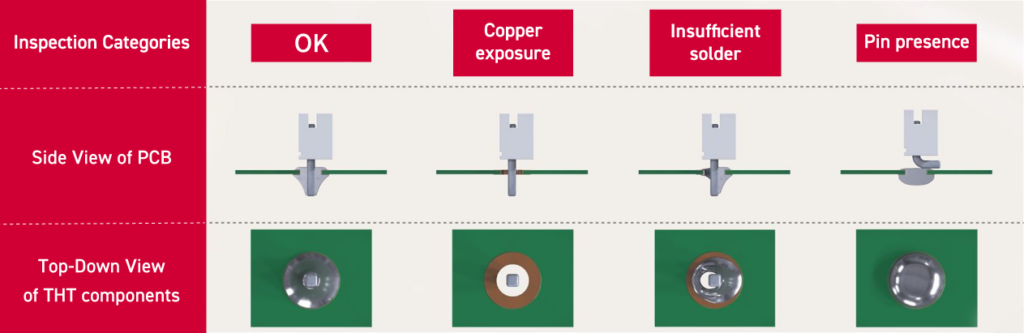
- THT solder inspection detects several solder defects simultaneously
- Extra Component Detection (ECD) inspection capability
The Bottom-Side AOI inspection capabilities cover a range of solder defects, essential for use by automotive manufacturers.
Dedicated ‘FUJIYAMA’ algorithm for THT solder joint and pin inspection
SAKI’s unique lighting technology enables analysis of solder meniscus and pin presence, allowing for the following defects to be simultaneously inspected:
• Copper exposure
• Excessive solder
• Pin presence
• Insufficient solder
• Blow holes
• Solder bridges
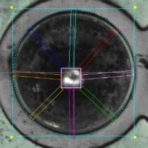
Through-Hole Solder Image
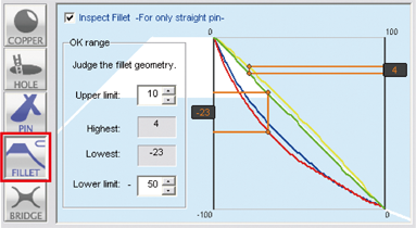
Through-Hole Solder Inspection Screen
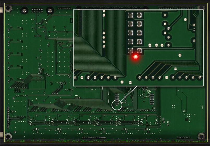
Extra Component Detection (ECD) inspects entire board without missing solder balls
ECD compares a non-defective statistical image with the newly scanned image allowing for the automatic detection of defects such as solder balls and foreign objects. This process also detects additional defects such as unexpected surplus parts and dust inside the board.
Statistical Template
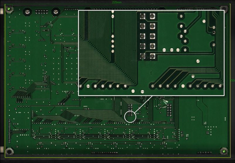
Defective PCB Assembly
Specification
2Di-LU1
Specification
| Model | 2Di-LU1 |
|---|---|
| Size (W)×(D)×(H)mm (in.) | 1040×1440×1500 (40.94 x 56.69 x 59.06) |
| Resolution | 18μm |
| PCB Clearance | Top: 130mm (1.57 in.) Bottom: 40mm (2.36 in.) |
| Electric Power Requirement | Single-phase ~ 200-240V +/-10%, 50/60Hz, 700VA |
| Weight | Aprox. 750kg |
| PCB Size (W)×(L)mm (in.) | Carrier:50 x 60 – 610 x 610 (1.97 x 2.36 – 24.02 x 24.02) Inspection area (Scan):50 x 60 – 460 x 500 (1.97 x 2.36 – 18.11 x 19.69) |
| PCB Weight | 12kg or less |