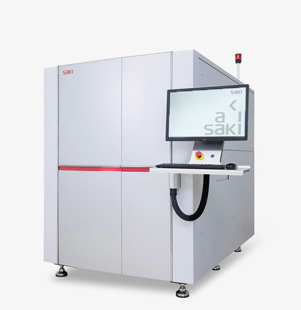
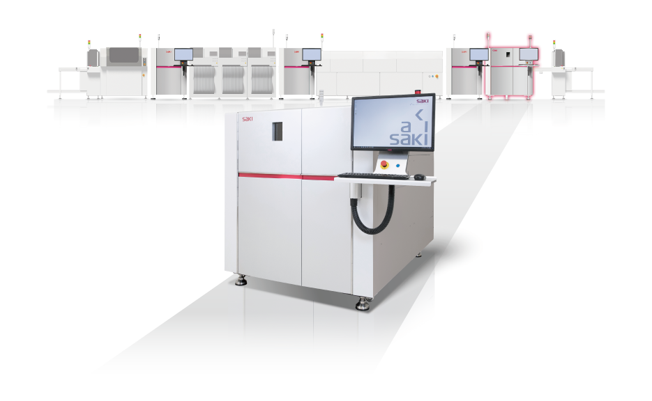
Inline 3D-CT Automated X-ray Inspection Systems
3D-CT AXI
A high-speed, high-precision 3D-CT X-ray inspection system, compatible with SMT, through-hole processes and Semiconductor inspection process, Saki’s 3D CT-AXI boasts the industry’s fastest speed, utlilizing superior 3D imaging and inspection quality to detect the full spectrum of solder defects on PCBs.
Our 3D-CT AXI include high-definition models and high-power, high-speed models to meet a variety of inspection requirements.
Example of Defect Detection Using High-Definition Image Aquisition
Head in Pillow
Void Defect
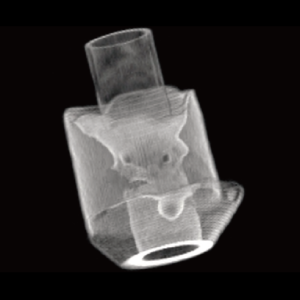
PTH Solder Defect
01

Powerful High-Speed, High-Definition Imaging
- The industry’s fastest imaging and calculation processing capability
- Detailed and true 3D image generation for zero-defect production
- Supports inspection of Slim and lightweight DSC power module

The industry’s fastest speed for inline inspection
An new, innovative larger detector for wide-area imaging results in fewer required FOVs and reduced takt time. When combined with Saki’s unique optimized software, imaging and calculation processing are completed almost simultaneously, producing the ultra-low cycle time required for efficient inline X-ray inspection.
High-definition 3D images
Saki’s unique Planar CT technology specializes in flat object imaging, instantaneously generating hundreds of high-definition tomographic images that are stiched together to create high-definition 3D data.
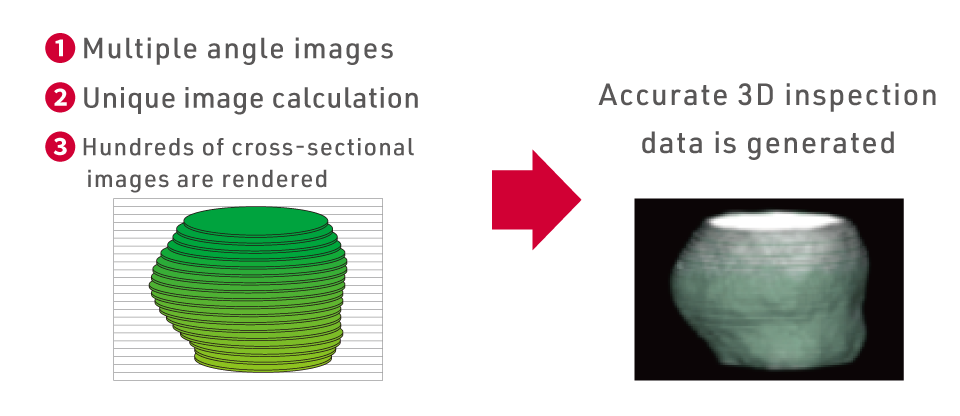
Saki’s high-precision hardware design is essential for the creation of high-definition 3D data. The ultra-rigid gantry and high-resolution linear scale provide incredible accuracy in positioning for stable imaging. Gantry position information is reflected in real-time calculations to obtain high-definition 3D images with clear edges.
High-precision correction technology
Generating high-definition 3D imagery requires high-precision correction technology. Saki’s 3D-AXI utilizes pattern data, an automatic board warp correction function in the XYZ directions, and a positioning function for improving inspection accuracy and to reduce the burden of creating inspection programs.
Seamless high-definition 3D data is acquired through a process that includes XYZ directional correction for each pixel combined with the 3D-AXI ‘One Piece’ function for connecting FOVs.
One Piece Function
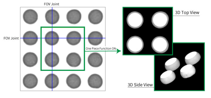
By combining high-precision imaging, correction, and calculation processing, it is possible to acquire dense 3D data based on the information in the X, Y and Z-axes – this ensures that defects are not overlooked at any height.
All inspections meet, or exceed, IPC standards.
General Inspection Method
Saki’s Inspection Method
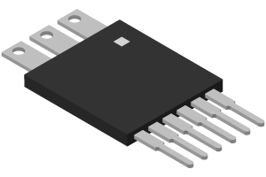
Supports inspection of Slim and lightweight DSC power module
By selecting X-ray tube with a maximum output of 130kV, it is also possible to inspect thin power modules.
The range of inspection objects expands from DSC power modules, chiplets, elements with aluminum cooling fins, to boards with transformers on the backside.
Not only does it improve penetration power, but it also improves brightness, shortening exposure times, and contributing to improved scanning speed. (Compared to standard tubes: Approx. 40% shorter)
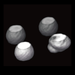
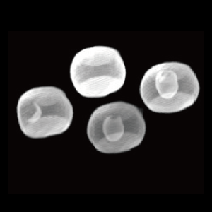
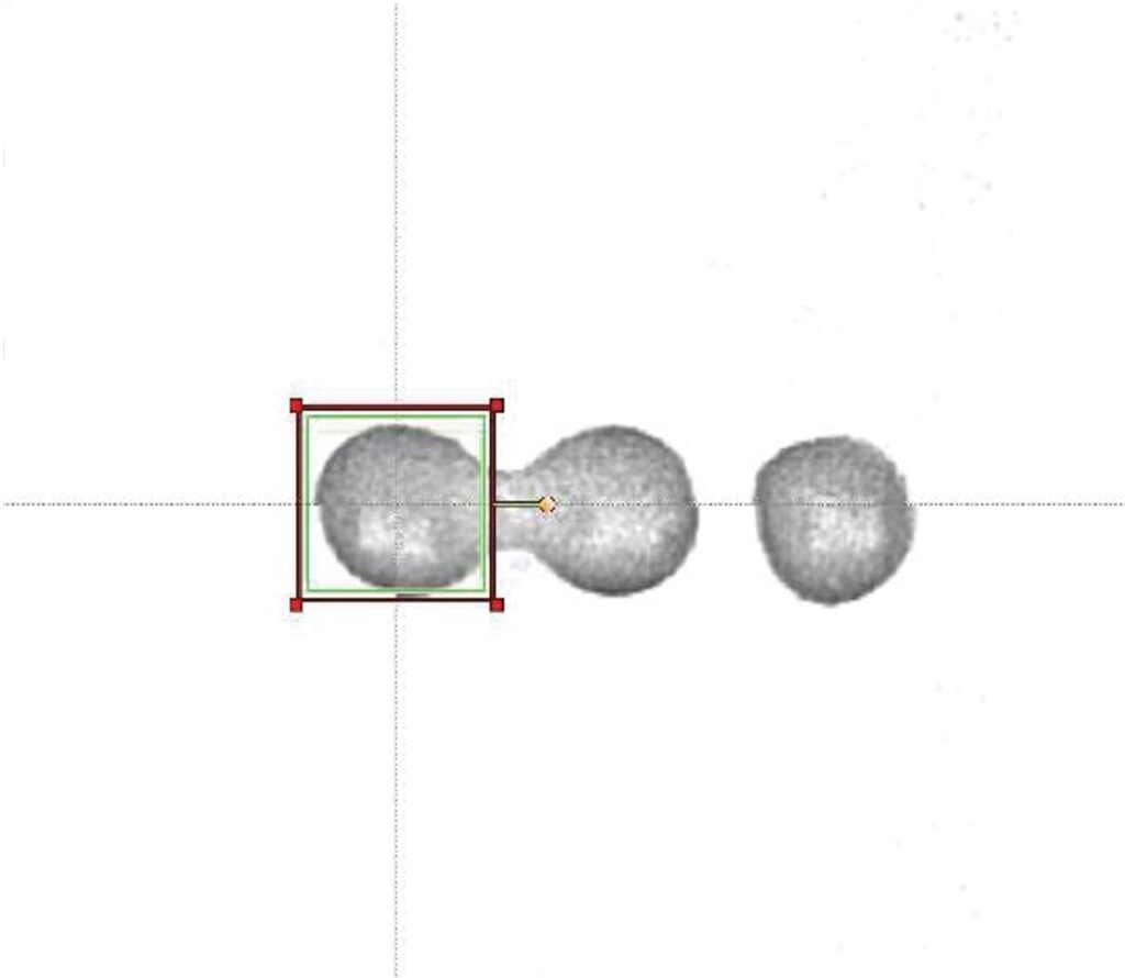
Slim and lightweight DSC power module
Saki’s 3Xi-M110 can clearly separate multi-layer components, such as spacers from multiple solder layers and also detect void defects.
Cross-sectional view of DSC power modules

02

Ease of Use and Reduced Workload
- Easy-to-program automatic imaging condition settings can be taken from AOI
- Debugging can be undertaken without stopping the production line
Easy programming
Inspection programs on conventional X-ray inspection machines can be difficult to create – in contrast, Saki’s X-ray inspection machines are able to draw from existing AOI programming data.
Programming time is significantly reduced by using pre-existing design data and by automatically setting imaging conditions, such as setting magnification for each FOV.
Additionally, parts that span multiple FOVs can be connected and saved as single-component 3D data for improved library management and reduced man-hours.
Debugging without halting the production line
The offline debugging function enables the collection and debugging of images without stopping the operating equipment. Alongside real-time library updates, a catalogue of historic defect data is saved and can be re-inspected, significantly contributing to overall quality assurance.
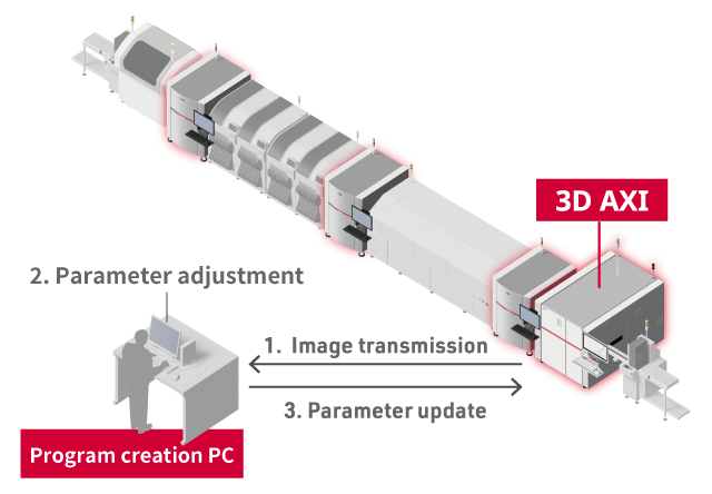
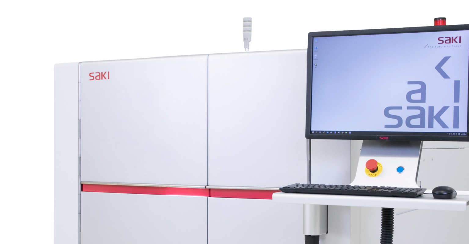
Advantages of cooperation with AOI
For ease of operability, Saki’s 3D-AXI inspection machine runs on the same software platform as its AOI. Achieving consistent quality control on the line, inspection results are integrated using both AOI and AXI – with results for each station displayed on the same screen. By sharing board ID information with the AOI, there is no need for intermediate conveyors or barcode readers, saving space and cost.
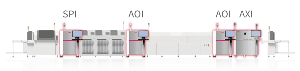
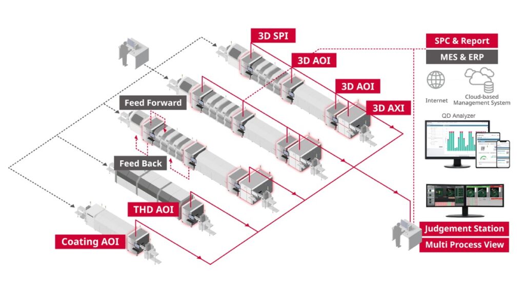
Saki’s Inspection Equipment Lineup for SMT Processes
03

Improved Maintainability and Ease of Maintenance
- Long-life hardware design for consistently high accuracy
- Self-diagnostic function, with exposure dose prediction and reduction
Future-proof hardware design
Highly-durable hardware is essential to perform advanced inspections while maintaining stable accuracy in inline, long-term high-volume production environments. Saki’s X-ray inspection machine has a unique highly-rigid gantry that achieves long equipment life and high repeatability.
Self-diagnostic functions
Sustaining high-precision, high-accuracy inspection is important to maintain high productivity. Saki’s X-ray inspection equipment regularly diagnoses the deterioration of the X-ray source, uneven image brightness, frame distortion, and more. Maintenance can be carried out in a planned manner and high-accuracy can be maintained. Self-diagnosis prevents sudden equipment failure, reduces equipment downtime, prevents unnecessary replacement of non-defective parts, and reduces maintenance man-hours.
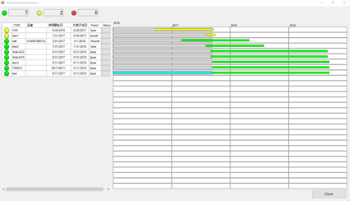
Time Based Maintenance
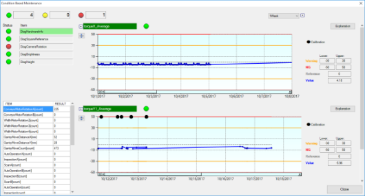
Condition Based Maintenance
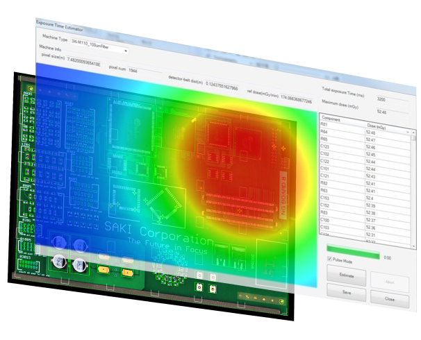
X-ray dosage simulator
When performing X-ray inspections, many people are concerned about the risk of component failure due to radiation exposure. Saki’s X-ray inspection equipment is equipped with an exposure dose simulator, predicting the exposure dose for each area to optimize imaging conditions. X-rays are irradiated only during imaging, minimizing irradiation.
X-ray Dosage Simulator
Optimal Functions for Each Process
SMT
- Example of SMT Process Defect Detection
Backend
- Example of defect detection in backend process
- SAKI’s total lineup solution
Example of SMT Process Defect Detection
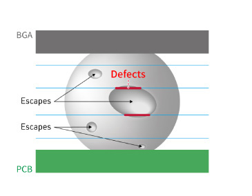
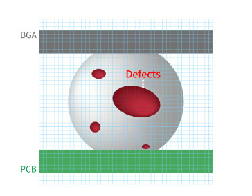
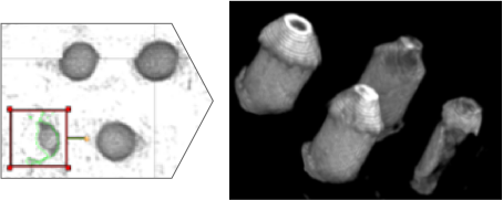
BGA Head in pillow
The 3D-AXI clearly separates unwetted shapes traditionally difficult to detect, performing inspection using the volume ratio and shape of solder balls.
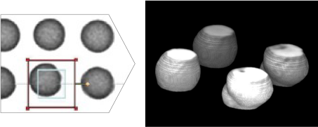
BGA Void Defect
The automatic inspection of both void volume ratio and void area ratio ensures that no voids, no matter how small, are overlooked.
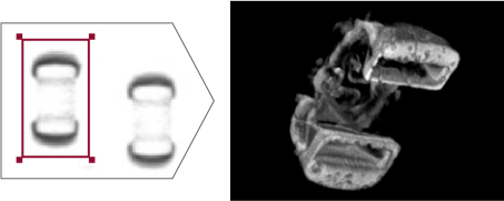
IC Components Solder Defect
Pass / fail judgments are based on changes in fillet position, height, width, angle, and number of IC components. If solder crosses between leads, it is detected as a bridge defect.
Chip Components Solder Defect
Pass / fail judgments are based on changes in fillet position, height, width, angle, and number of chip parts.
Example of defect detection in backend process
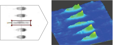
Insertion Part: Insufficient Solder Filling
The 3D-AXI measures the solder filling rate inside the through-hole and reliably detects defects that are missed by general tomographic image area inspection.
All inspections meet, or exceed, IPC standards.
Insertion Part: Faulty Bridge
If solder crosses between the leads, it is detected as a bridge defect.
SAKI’s total lineup solution
SAKI’s 3D AOI uses a common platform with 3D SPI and 3D CT AXI.
We can cover everything from post-printing solder inspection using SPI to inspection of mounted components with a consistent operation.
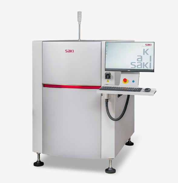
Specification
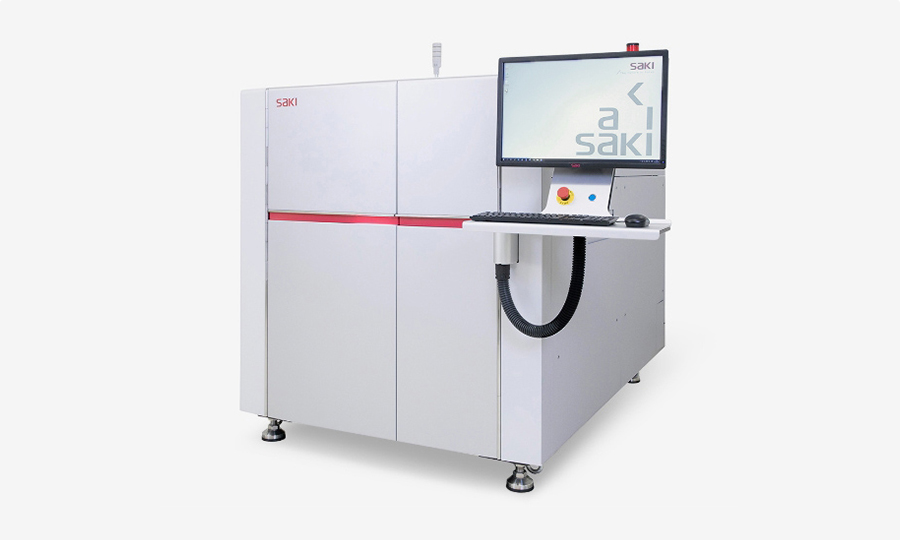
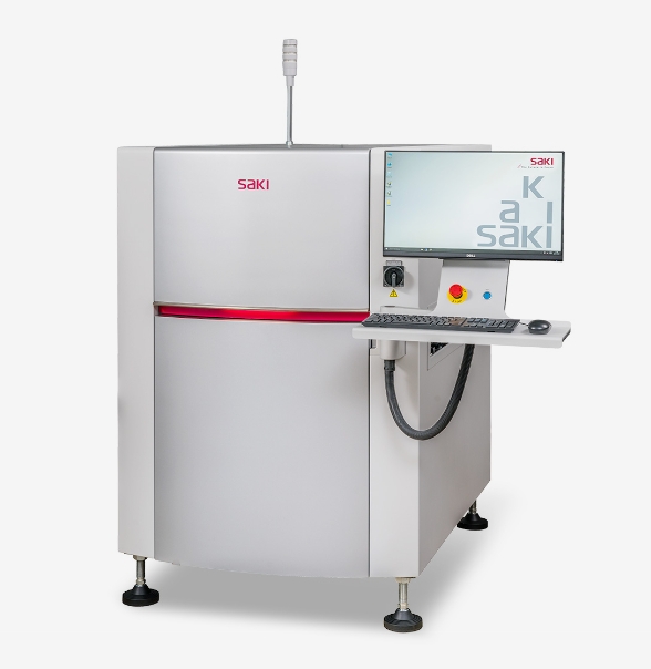
3Xi-M110
Specification
| Model | 3Xi-M110 | |
|---|---|---|
| X-ray Tube | 110kV 30W, Closed X-ray Source | 130kV 39W, Closed X-ray Source*1 |
| Size (W)×(D)×(H)mm (in.) | 1380×2166×1500 (54.34 x 85.28 x 59.06) | |
| Resolution | 8μm-38μm | 12μm-40μm |
| PCB Clearance | Top: 60mm(2.36 in.) Bottom: 40mm(1.57 in.) | |
| Electric Power Requirement | Three Phase 200-240V ±5 %, 50/60Hz | |
| X-ray Leakage | 0.5μSv/h or less | |
| PCB Size (W) x (L) mm (in.) | 50 x 120 – 360 x 330 (1.97 x 4.73 – 14.17 x 12.99) 50 x 120 – 360 x 510 (1.97 x 4.72 – 14.17 x 20.07) *2 | |
| Weight | Aprox. 3,100kg | |
| Model | 3Xi-M110 V3 |
|---|---|
| X-ray Tube | 110kV 30W, Closed X-ray Source |
| Size (W)×(D)×(H)mm (in.) | 1380×2166×1500 (54.34 x 85.28 x 59.06) |
| Resolution | 8μm-38μm |
| PCB Clearance | Top: 60mm(2.36 in.) Bottom: 40mm(1.57 in.) |
| Electric Power Requirement | Three Phase 200-240V ±5 %, 50/60Hz |
| X-ray Leakage | 0.5μSv/h or less |
| PCB Size (W)×(L)mm (in.) | 50 x 120 – 360 x 330 (1.97 x 4.73 – 14.17 x 12.99) 50 x 120 – 360 x 510 (1.97 x 4.72 – 14.17 x 20.07) *2 |
| Weight | Aprox. 3,100kg |
| Model | 3Xi-M110 V4 |
|---|---|
| X-ray Tube | 130kV 39W, Closed X-ray Source*1 |
| Size (W)×(D)×(H)mm (in.) | 1380×2166×1500 (54.34 x 85.28 x 59.06) |
| Resolution | 12μm-40μm |
| PCB Clearance | Top: 60mm(2.36 in.) Bottom: 40mm(1.57 in.) |
| Electric Power Requirement | Three Phase 200-240V ±5 %, 50/60Hz |
| X-ray Leakage | 0.5μSv/h or less |
| 対象基板サイズ (W)×(L)mm | 50 x 120 – 360 x 330 (1.97 x 4.73 – 14.17 x 12.99) 50 x 120 – 360 x 510 (1.97 x 4.72 – 14.17 x 20.07) *2 |
| Weight | Aprox. 3,100kg |
*1 A high power X-ray tube (130kV) is optional item.
*2 Target board size with 2x imaging option
Use Case

Marquardt
Marquardt, a leading German manufacturer of mechatronic products for the automotive industry, has installed Saki’s 3D-AOI and 3D-CT-AXI solutions to improve production efficiency and ensure their competitiveness in the future.
Related Solutions
3D-SPI
3D Solder Paste
Inspection Machine
3D-AOI
3D Automated Optical Inspection Systems
Power Module-AXI
Inline 3D X-ray Inspection Machine for IGBT Power Modules