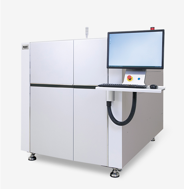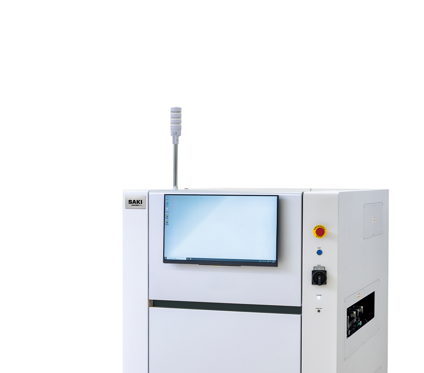
3D Automated Optical Inspection
Systems
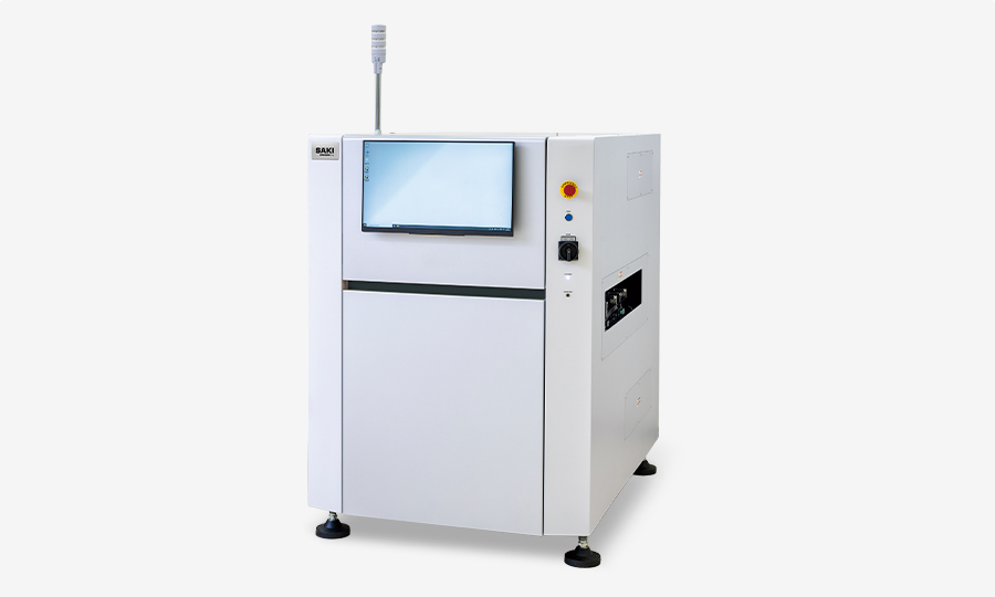
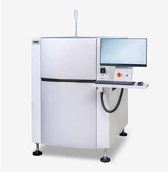
3D-SPI / 3D-AOI
GX Series
SAKI’s 3D-SPI enable increased production efficiency with remarkable speed, as well as increased product and performance quality and takt-time control. Fully compatible with both SMT and through-hole processes, the 3D-AOI meets all quality requirements for complex inspection targets, such as high-density printed circuit boards and boards housing a mix of both extremely small and tall components.
01

3D-SPI
- High-accuracy, high-quality and versatile solder print inspection
- The industry’s fastest speed for inline inspection
- M2M collaboration to realize line automation

IPC-compliant inspection quality
Positional deviation of pad size is inspected based on the IPC-7527 quality standard for measurement allowances.
IPC-7527 Quality Standard Inspection
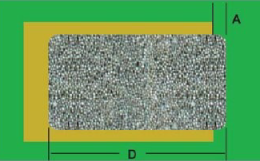
Printing Deviation Standard
Paste solder protruding from the pad Class 1,2,3: less than 25%
Actual Image
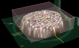
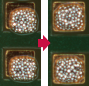
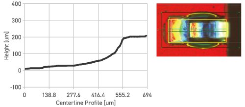
Coplanarity inspection
High I/O count device inspections benefit from improved coplanarity, with solder range analysis for height, volume, area that helps prevent post-reflow wetting.

Coordination with Printer – Feed-back from SPI to screen printer –
SPI feeds back misalignment data, preventing print errors and triggering automatic stencil cleaning alerts.
Correction of the Print Position
Automatic Cleaning Instructions
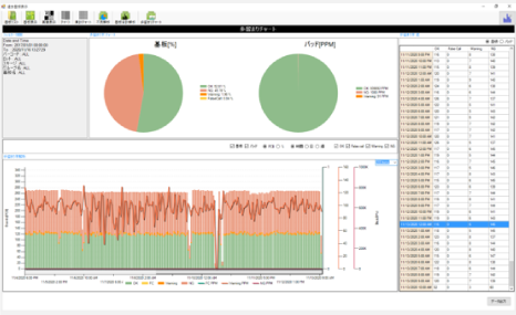
SPC functions for visualization of solder quality
Solder quality is managed and maintained through comprehensive monitoring of board solder amounts and defect trend analysis. Extensive reporting functions and data analysis tools allow for export of defect type rankings and yield charts.
Defect Analysis
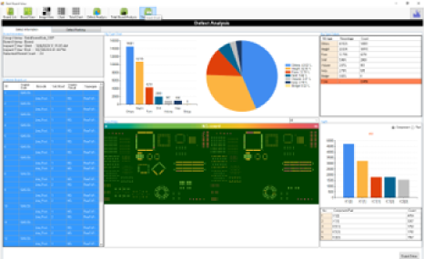
Yield Chart
02

3D-AOI
- High-precision and high-speed inspection
- Increased work efficiency for inspection programs creation
- Reducing reliance on operator skill with AI solutions
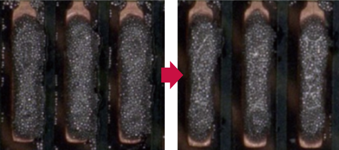
Solder Fillet Inspection
“Fillet Shape” Solder Inspection Algorithm supports the inspection of various types of components and enables solder fillet inspection in compliance with IPC inspection standards.
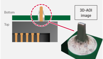
THT Solder Inspection
The FUJIYAMA solder inspection algorithm has been upgraded. In addition to the inspection of pins, holes, and solder fillets, further functions now also inspect for overabundance excessive solder.
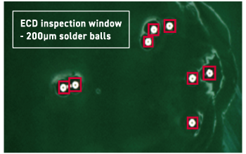
Full Surface Inspection for Foreign Objects & Solder Balls
This feature detects foreign bodies and fallen objects across the entire board. With the latest software, solder ball detection tests can be conducted across the entire board simultaneously with normal foreign object inspection.
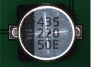
OCR Inspection
Achieves high-precision inspection of characters and polarity on components with a maximum component height of 10mm. By focusing on both the board surface and the component surface, solder inspection and character polarity inspection can be performed simultaneously.
Conformal Coating Inspection (CCI) possible with UV lighting*
CCI detects coverage / non-coverage areas on the entire PCB.
Extra Component Detection (ECD) is also possible.
*Optical unit for UV lighting optional.
Offline Debugging
In a mass production environment, this feature visualizes operator assessment results (false calls, NG) and adjusts inspection parameters accordingly.
03
Advanced Software Solutions
- Unified user interface across SPI, AOI, and AXI
- Increased work efficiency for inspection program creation
- Enhanced production with AI solutions with improving inspection quality
Easy Programming
・Decrease programming time and effort with automated creation of inspection program
・Eliminate programming errors with comprehensive automated inspection data creation
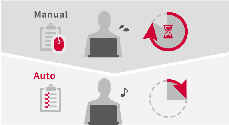
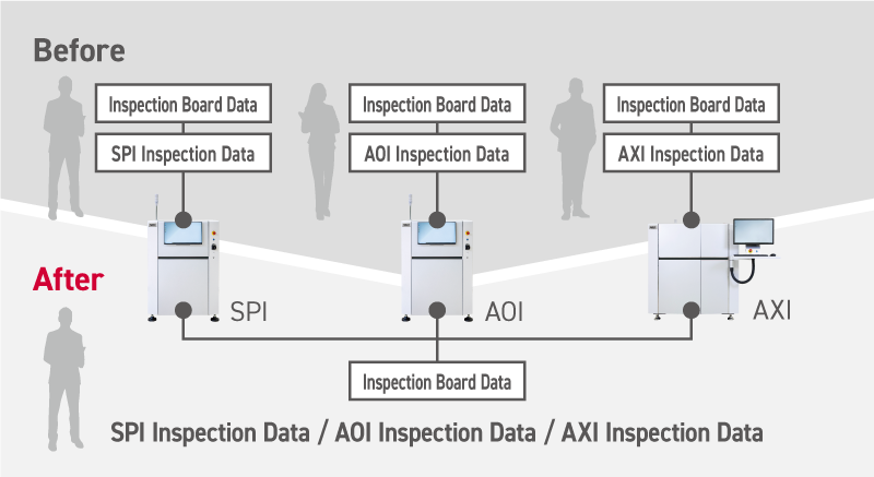
One Programming
Standardized inspection program data for SPI, pre-AOI, and post-AOI, eliminates duplicate tasks and reduces line setup by approximately 30%.
Saki Link
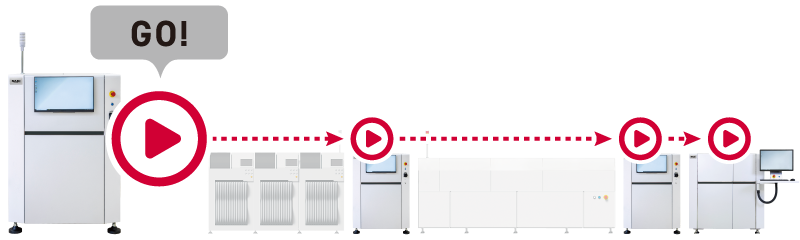
One Operation Control
Load a single inspection program to start/stop all connected devices automatically.
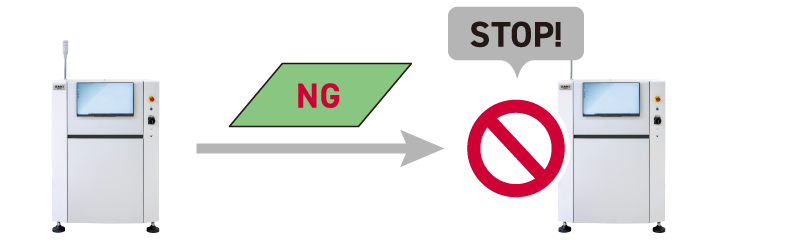
Process Check
Prevent defective boards from moving to post-processing, if an upstream inspection machine flags a board as NG, it is marked as an “Operation Error”.
Bad Board Skip Function
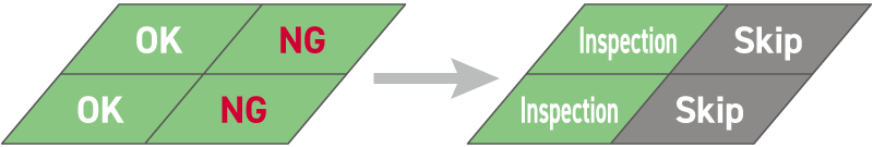
Reduces X-ray inspection time by sharing AOI inspection results with the X-ray system, enabling bad-marked boards to be skipped.
AI solutions
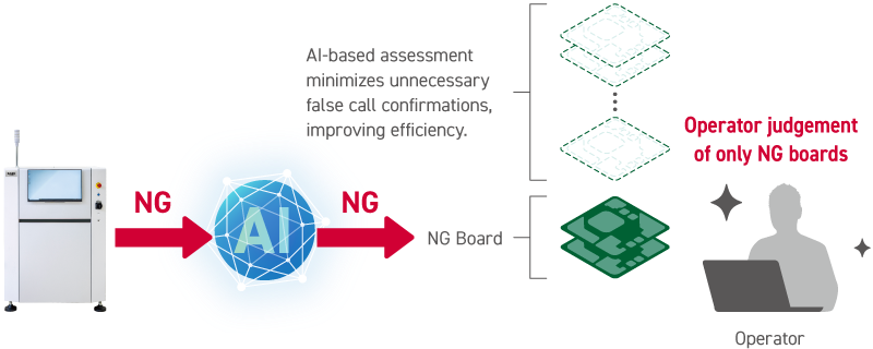
AI Assist : Uses AI to re-assess, reducing operator workload.
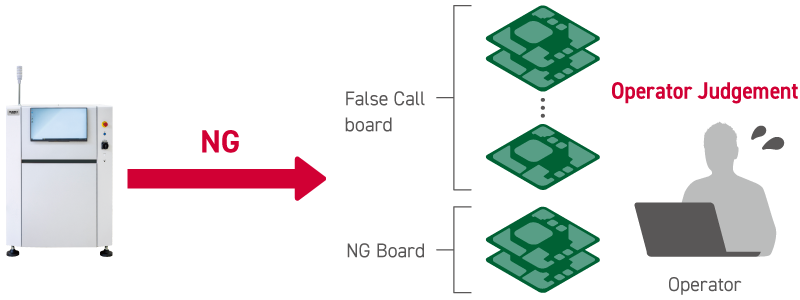
In the conventional judgment, parts that were judged to be NG by the inspection machine were re-judged by the operator on the judgment monitor. For AI assist, the AI performs a re-judgment before the operator judgment for inspection NG parts. AI significantly reduces manual confirmation workload, requiring operators to visually inspect only AI-determined NG parts.
Conventional judgment
Operators have to verify each component flagged as NG (No Good) by the inspection machine, which can be labor-intensive and is prone to errors and misjudgment.
Judgment after introduction of AI assist
AI performs a second assessment on parts marked NG, drastically reducing the operator’s workload by requiring manual verification only for AI-determined NG parts. This system helps prevent overlooked errors caused by misjudgment.
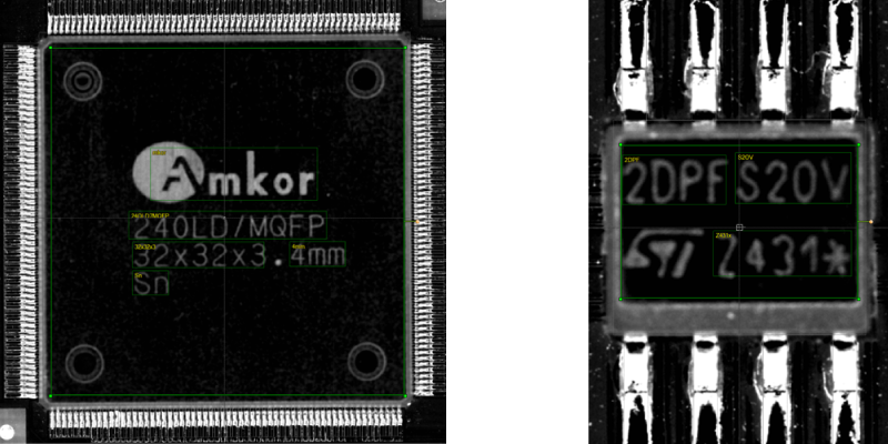
AI Inspection (AI OCR)
AI OCR detects and recognizes characters dynamically.
In the traditional matching-based character inspection, the operator adjusted the parameters every time in order to respond to variations in print position, uneven surfaces, part substitutions, and variations in manufacturer markings.
AI algorithm inspection enables stable testing regardless of print misalignments or font variations, bridging the skill gap and ensuring consistent inspection quality.
Specifications
3Si-LS3GX / 3Di-LS3GX
| Model | 3Si-LS3GX | 3Di-LS3GX |
|---|---|---|
| Dimensions | L | |
| Size[Main body] (W) x (D) x (H) mm (in.) | 1040×1280×1500 (40.95 x 50.39 x 59.06) | |
| Resolution | 15μm | |
| PCB Clearance mm (in.) | Top: 40 (1.57) Bottom: 60 (2.36) | |
| Electric Power Requirement | Single-phase ~ 200-240V+/-10%, 50/60Hz | |
| PCB Size (W)×(L)mm (in.) | 50 x 60 – 510 x 510 (1.97 x 2.36 – 20.07 x 20.07) | |
| Model | 3Si-LS3GX |
|---|---|
| Dimensions | L |
| Size[Main body] (W) x (D) x (H) mm (in.) | 1040×1280×1500 (40.95 x 50.39 x 59.06) |
| Resolution | 15μm |
| PCB Clearance mm (in.) | Top: 40 (1.57) Bottom: 60 (2.36) |
| Electric Power Requirement | Single-phase ~ 200-240V+/-10%, 50/60Hz |
| PCB Size (W)×(L)mm (in.) | 50 x 60 – 510 x 510 (1.97 x 2.36 – 20.07 x 20.07) |
| Model | 3Di-LS3GX |
|---|---|
| Dimensions | L |
| Size[Main body] (W) x (D) x (H) mm (in.) | 1040×1280×1500 (40.95 x 50.39 x 59.06) |
| Resolution | 15μm |
| PCB Clearance mm (in.) | Top: 40 (1.57) Bottom: 60 (2.36) |
| Electric Power Requirement | Single-phase ~ 200-240V+/-10%, 50/60Hz |
| PCB Size (W)×(L)mm (in.) | 50 x 60 – 510 x 510 (1.97 x 2.36 – 20.07 x 20.07) |
Related Solutions
3D-SPI
3D Solder Paste
Inspection Systems
3D-AOI
3D Automated Optical Inspection Systems
3D-CT AXI
Inline 3D-CT Automated
X-ray Inspection Systems