SAKI Launches New Inline 3D Bottom-Side AOI System
Advanced back-end inspection solution combines high-precision THT solder inspection with automated full-surface PCB inspection – without board flipping
Tokyo, Japan – October 15, 2026 – SAKI Corporation, an innovator in the field of automated optical and X-ray inspection equipment, is pleased to announce the launch of its new 3Di-LS3BX inline 3D bottom-side automated optical inspection (AOI) system. Designed to automate back-end PCB inspection following selective, wave, and dip soldering processes, the latest AOI system combines high-precision inspection of through-hole technology (THT) solder joints with simultaneous full-surface inspection, eliminating the need for PCB flipping and reducing manual handling requirements.
As quality assurance requirements become increasingly demanding, particularly in automotive electronics and other high-reliability applications, manufacturers face growing pressure to maintain consistent inspection quality while improving production efficiency. Conventional back-end inspection processes often require additional board handling or manual intervention, increasing operational complexity and the potential for handling-related damage.
The 3Di-LS3BX machine addresses these challenges by enabling automated bottom-side inspection directly within the production line, supporting consistent inspection quality while reducing operator intervention and the risk of human error.
High-Precision 3D Inspection of THT Solder Joints
The 3Di-LS3BX combines dedicated THT solder inspection software, SAKI’s proprietary inspection algorithms, and precise 3D measurement to deliver stable and reliable inspection of component pins and solder fillets.
SAKI’s proven high-rigidity gantry structure ensures stable inspection performance and excellent repeatability, while standard dome lighting supports consistent 3D imaging of sloped, reflective, and curved surfaces. Together, these technologies enable high-precision inspection while significantly reducing false calls.
Simultaneous Full-Surface Inspection with Full Memory Technology
In addition to standard component and solder fillet inspection, SAKI’s proprietary Full Memory Technology enables simultaneous inspection of solder balls and foreign object debris (FOD) across the entire PCB, including unexpected components.
The system can detect solder balls down to 200 µm, providing an additional level of inspection coverage for potential defects that might otherwise remain undetected during conventional inspection processes.
Seamless Integration into Existing Inspection Environments
The 3Di-LS3BX uses the same software platform as SAKI’s solder paste inspection (SPI) and post-reflow AOI systems, providing a common operating environment and supporting standardized inspection workflows across SMT and back-end processes.
An optional return conveyor can also be installed beneath the system to accommodate different production line configurations and simplify integration into existing manufacturing environments.
With the introduction of the 3Di-LS3BX, SAKI further expands its inspection portfolio, providing manufacturers with integrated solutions that support consistent quality assurance throughout the production line, from SMT to back-end processes.
For more information about the 3Di-LS3BX, please visit the SAKI product information page.
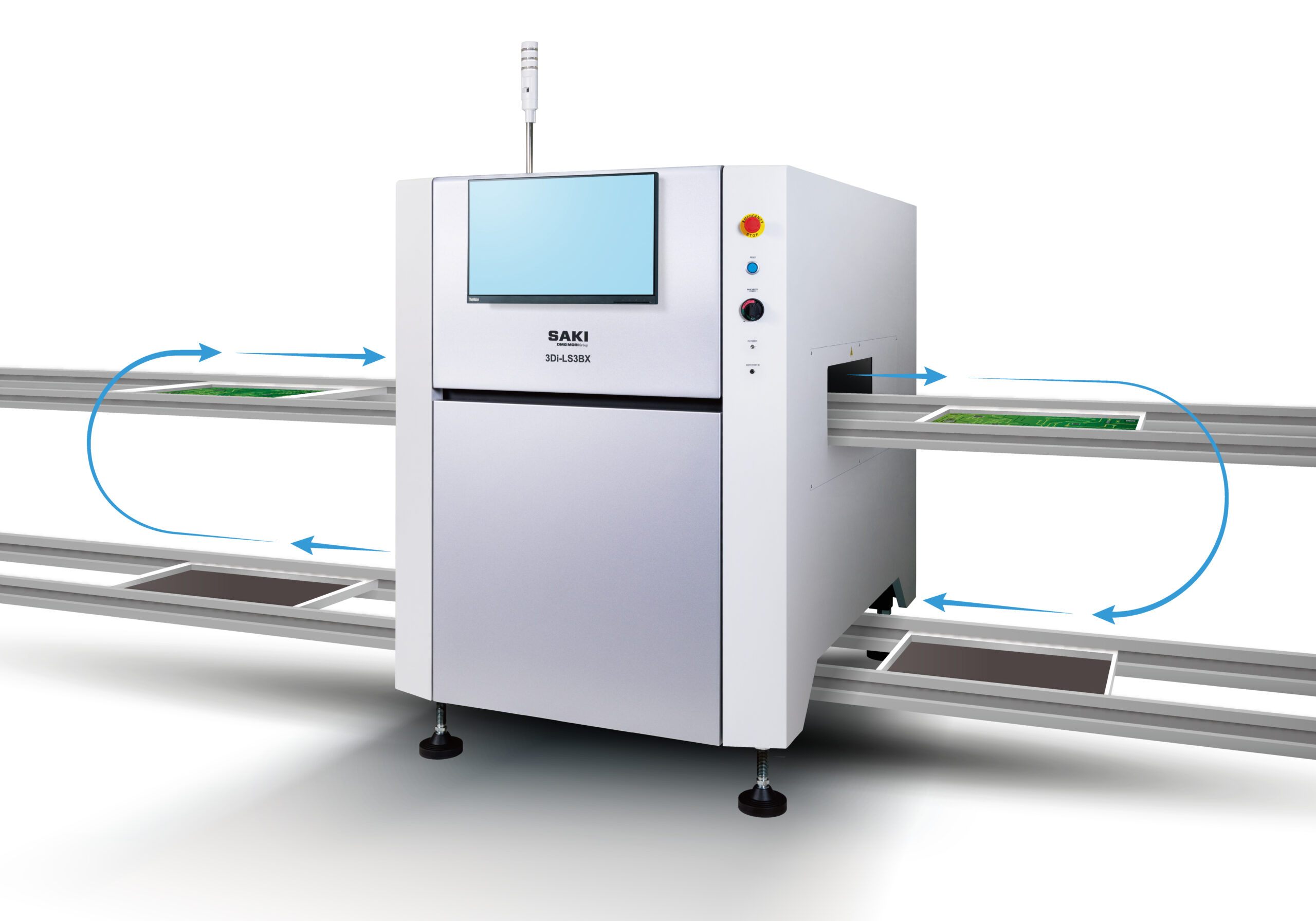
3Di-LS3BX Image