
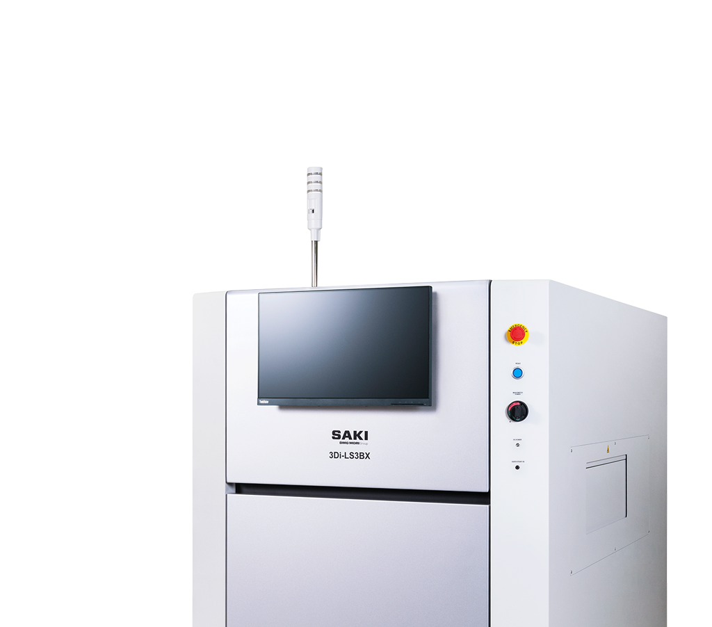
Inline Bottom-Side 3D Automated Optical Inspection System
Bottom-Side
3D-AOI
3Di-LS3BX – a bottom-side 3D-AOI system designed to automate final insprection in the PCB assembly process.
High-precision 3D inspection of the bottom-side of the PCB significantly reduces false calls while providing reliable inspection and quality of THT solder joints following selective, wave, and dip soldering processes.
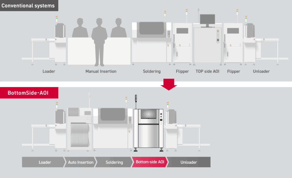
By eliminating the need for PCB flipping and additional board handling, the 3Di-LS3BX helps improve productivity, reduce the risk of PCB damage, and optimize production floor space.
01

Defect Detection Performance
- High-Precision Solder Fillet Inspection
- Full-Surface FOD Inspection for Reliable Solder Ball Detection
- Hardware Engineered for High-Accuracy Inspection

High-Precision Solder Fillet Inspection
An optimized THT solder inspection algorithm simultaneously detects a wide range of solder defects.
A single algorithm enables inspection of non-wetting, pinholes, solder bridges and other solder joint defects.
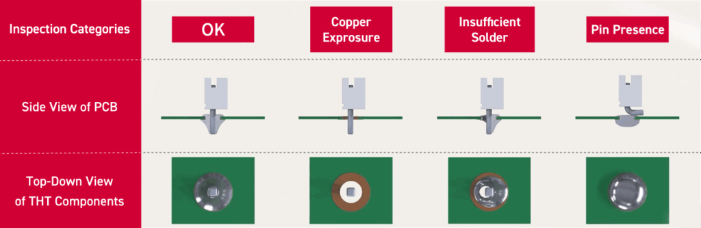
Improved Quality Through 3D Inspection
Precise 3D height data enables easy and reliable detection of defects that can be difficult to distinguish using 2D inspection, including excessive solder.
Accurate 3D measurement also enhances pin inspection accuracy.
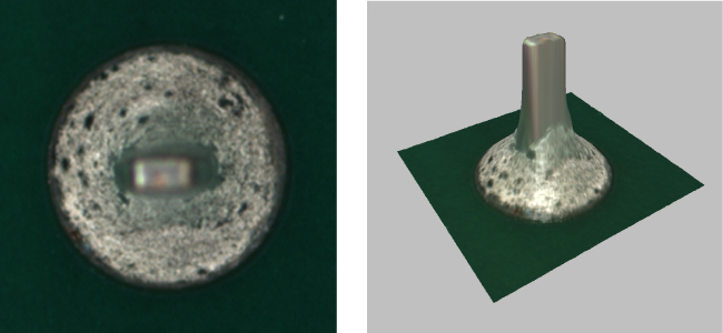
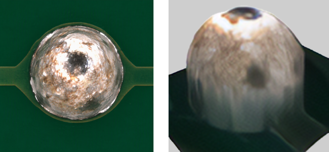
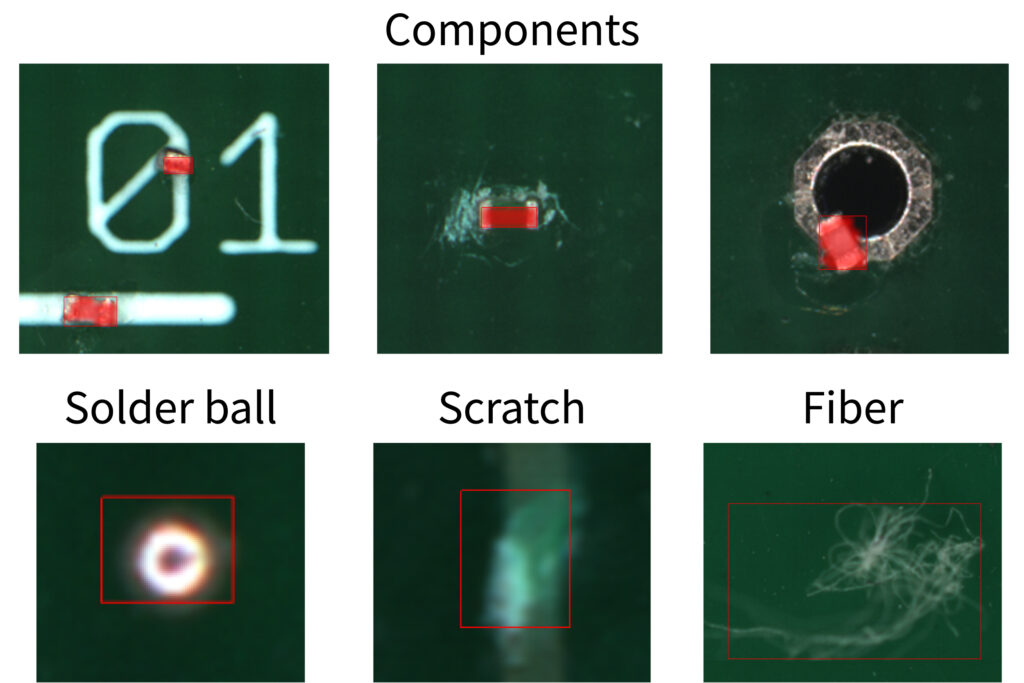
Full-Surface FOD Inspection for Reliable Solder Ball Detection (ECD)
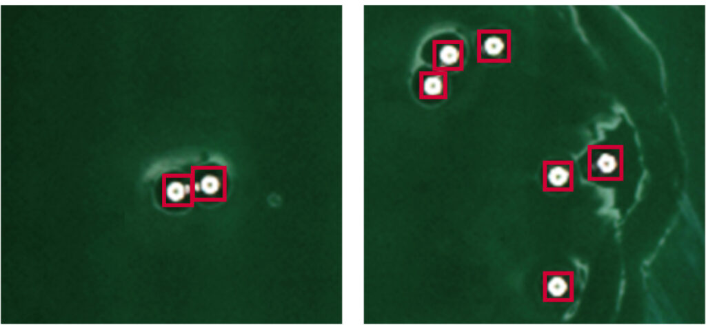
SAKI’s proprietary Full Memory Technology enables simultaneous inspection of solder balls and foreign object debris (FOD) across the entire PCB, including unexpected components. The 3Di-LS3BX can detect solder balls down to 200 µm.
Solder ball ECD window
ECD inspection window – 200µm solder balls
Examples of surplus components
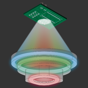
Hardware Engineered for High-Accuracy Inspection
SAKI’s proven high-rigidity gantry structure ensures stable inspection performance and excellent repeatability. Standard dome lighting enables stable 3D imaging of sloped, reflective, and curved surfaces, ensuring consistent, high-precision inspection.
02

Improved Production Efficiency
- Automated Bottom-Side Inspection for Greater Production Efficiency
- Hardware Configuration Optimized for Back-End Processes
Automated Bottom-Side Inspection for Greater Production Efficiency and Labor Optimization
Eliminating the need for PCB flipping and additional board handling reduces the risk of PCB damage. The removal of a board inverter requirement also reduces line length and equipment footprint, improving floor-space utilization and production efficiency.
Hardware Configuration Optimized for Back-End Processes
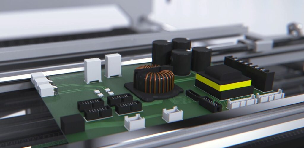
With 140 mm top-side clearance and a high-rigidity conveyor, the 3Di-LS3BX accommodates PCBs with large odd-form/THT components as well as heavy fixtures, expanding the range of back-end inspection processes that can be automated.
Large, Odd-Shaped Inserted Component Mounted PCBs
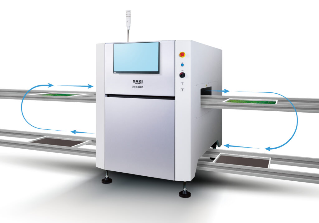
The machine is designed to accommodate a return conveyor beneath the machine, enabling flexible production line configurations.
03

Reduced Operational Workload
- Common Software Platform Across SAKI Inspection Systems
- Automatic Inspection Data Creation
- Self-Diagnostic Function
Common Software Platform Across SAKI Inspection Systems
The 3Di-LS3BX uses the same software platform as SAK’s solder paste inspection (SPI) and post-reflow automated optical inspection (AOI) systems.
A common operating environment standardizes workflows and reduces operator workload.
Automatic Inspection Data Creation
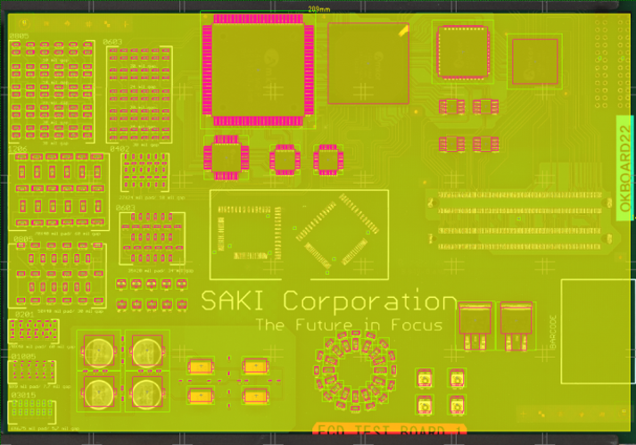
Inspection data is automatically generated from solder mask Gerber data, significantly reducing programming time and operator workload while enabling faster system setup.
Self-Diagnostic Function
Built-in self-diagnostic functionality automatically monitors system status, supporting efficient preventive maintenance and stable, reliable operation while helping maintain inspection accuracy.
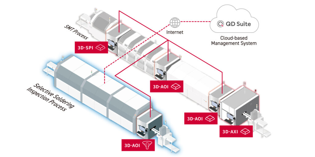
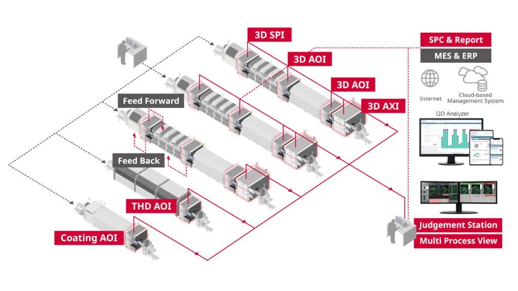
SAKI’s Total Lineup Solution
SAKI’s 3D-AOI uses a common platform with 3D-SPI and 3D-CT-AXI. The process is consistent throughout – from post-printing solder inspection using SPI, through to the inspection of mounted components.
Specification
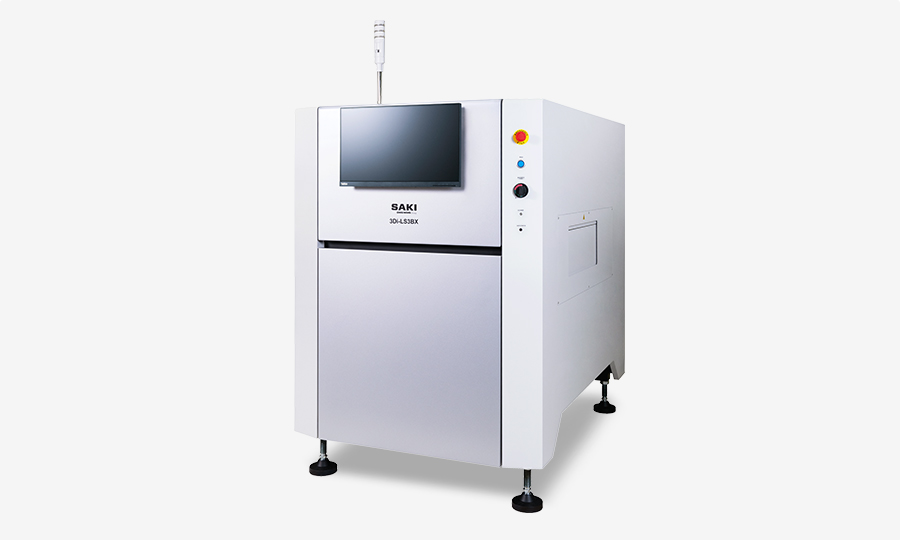
3Di-LS3BX
| Model | 3Di-LS3BX |
|---|---|
| Size (W)×(D)×(H)mm(in.) | 1,140×1,700×1,580 (44.88×66.93×62.20) |
| Resolution | 15μm |
| PCB Clearance | Top: 140mm(5.51 in.)/Bottom: 35mm(1.38 in.) |
| Electric Power Requirement | Single phase to 200-240V±10%、50/60Hz、650VA 3.3A |
| Weight | Approx. 980kg |
| PCB Size (W)×(L)mm(in.) | 50×100-510×510 (1.97×3.94-20.08×20.08) 50×100-510×720 (1.97×3.94-20.08×28.35)*1 |
| PCB Weight | For PCB conveyor rail:2㎏ or less For weight transfer conveyor rail:12㎏ or less |
(*1) PCB size for the two-step scan function.