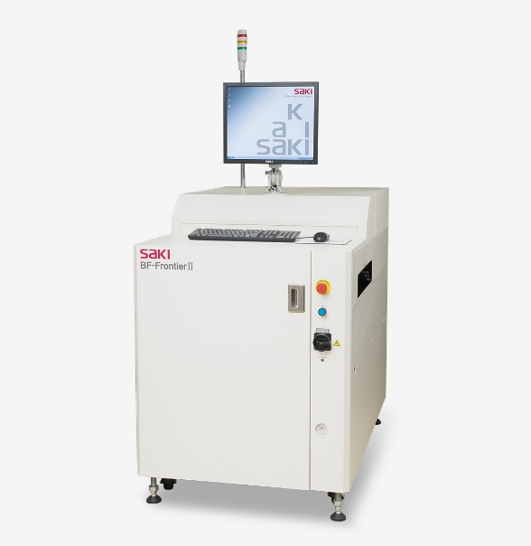
3D Automated Optical Inspection
Systems
3D-AOI
Fully compatible with both SMT and through-hole processes, the 3D-AOI meets all quality requirements for complex inspection targets, such as high-density printed circuit boards and boards housing a mix of both extremely small and tall components. The camera resolution and lighting are customizable to provide the flexibility to suit any production environment or product range.
01

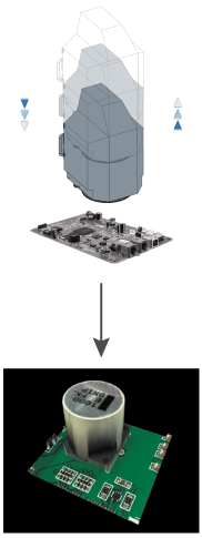
Scalability
- Multiple options available, including: dome lighting, side camera, Z-axis
- Conformal Coating Inspection (CCI) possible with UV lighting option

Upgradeable options enable a variety of board inspections with a single inspection machine
Upgrades enable continuous up-to-date performance and a wider range of inspection use from a sole unit.
Dome Lighting
Side Cameras
Z-Axis
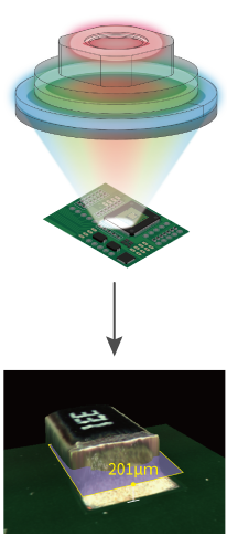
Conformal Coating Inspection (CCI) possible with UV lighting*
CCI detects coverage / non-coverage areas on the entire PCB.
Extra Component Detection (ECD) is also possible.
*Optical unit for UV lighting optional.
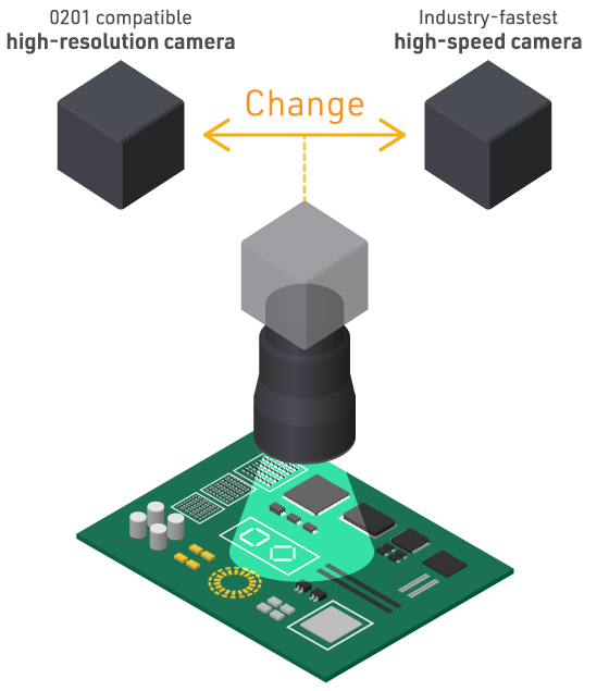
On-site switching of camera resolution
Both resolution and speed can be switched according to the inspection target and production requirements.
Changeover can be completed in less than 90 minutes – including on-site calibration.
02

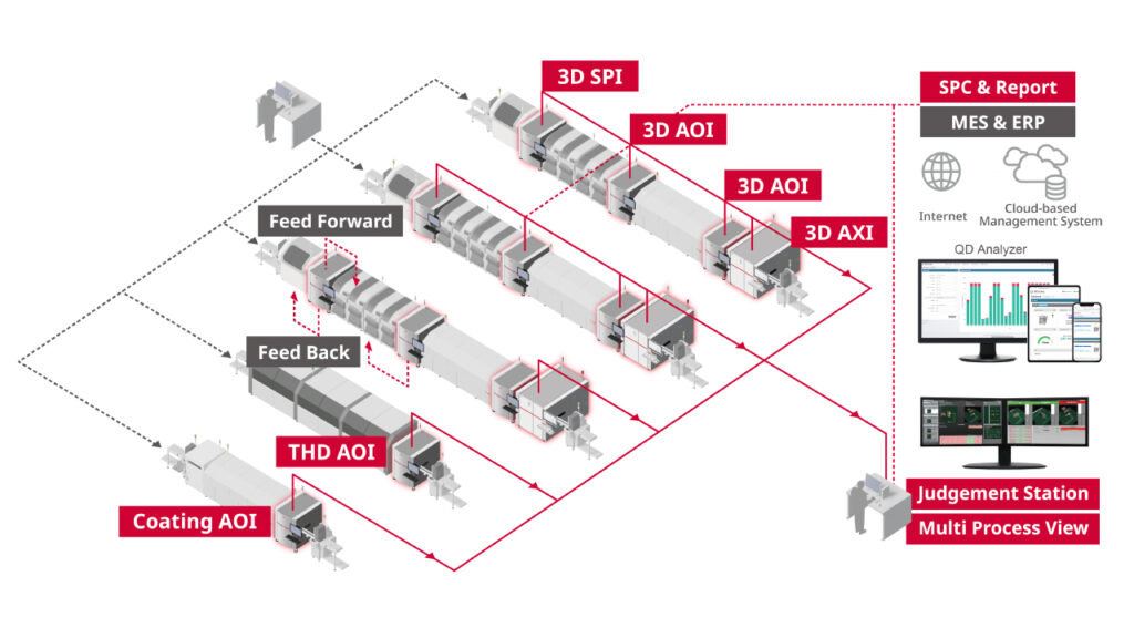
Optimization of the production line
- Automation and efficiency of inspection program creation
- Seamless coordination between Saki Devices
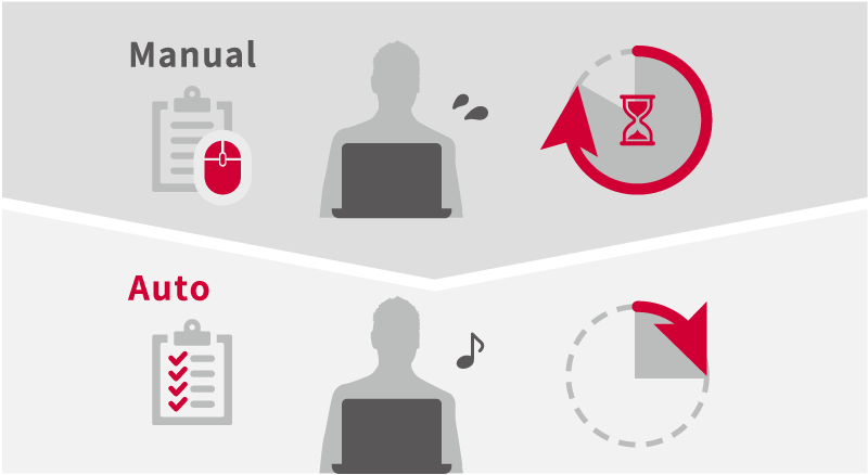
Easy Programming
・Cut programming time and effort with automated inspection program development tools
・Eliminate programming errors with comprehensive automated inspection data creation
One Programming
Standardized inspection program data for SPI, pre-AOI, post-AOI, and AXI eliminates duplicate tasks and reduces line setup time to approximately one-third.
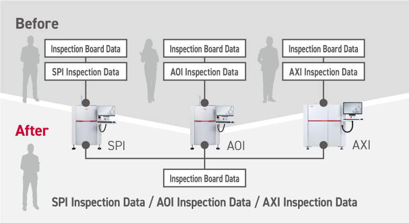
Saki Link
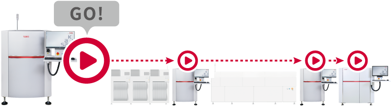
One Operation Control
Load a single inspection program to start/stop all connected devices automatically.
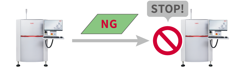
Process Check
Prevent defective boards from moving to post-processing, if an upstream inspection machine flags a board as NG, it is marked as an “Operation Error”.
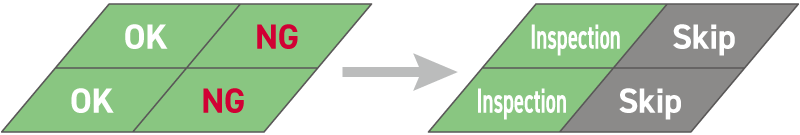
NG Board Skip Function
Reduces X-ray inspection time by sharing AOI inspection results with the X-ray system, enabling bad-marked boards to be skipped.
03

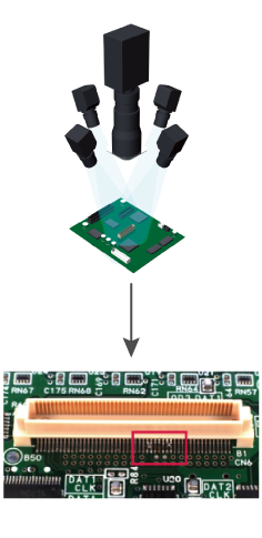
High accuracy and high speed
- Quality high-definition images clearly depict the smallest components
- Performs inspections at the quickest speed possible
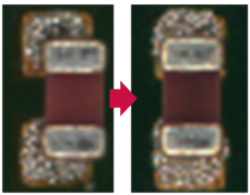
High-definition images presenting minute parts and high-density PCBs in stunning clarity
Able to accurately inspect a range of parts with extremely clear imagery, the 3D-AOI inspects 0402mm and 0201mm components, as well as detailing narrow pitch IC and narrow pad parts.
New AOI

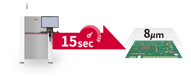
0402mm component captured on 3Di-LS3 / 8µm
Conventional AOI

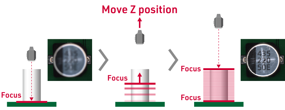
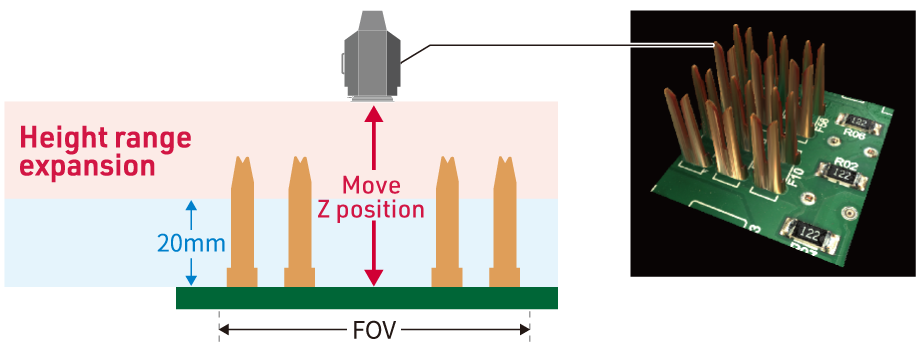
Achieving the impossible – high-resolution imagery with an expanded height measurement range
The 3D-AOI maintains high resolution while expanding the height measurement range, achieving comprehensive inspection of both extremely small-sized and tall components. The height measurement range is up to 25mm with the resolution 8µm / 15µm camera alone, and can be expanded to 40mm when combined with the Z-axis option.
Tall Components with SMT Process

Press Fit Components

Unparalleled AOI cycle times with both 8µm and 15µm resolution cameras
Enjoy speeds of 4,500mm²/sec with the 8µm camera and 7,000mm²/sec with the 15µm camera.
With the ability to handle components as small as 0402mm, the 15µm camera is ideal for high-volume products and those where speed is essential.
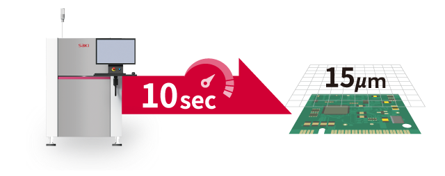
Combined capturing and inspection time totals with A5-size sample (150mm x 214mm)(inspection time may vary depending on sample condition)
High-speed image data processing
Imaging, image data processing, and inspection are all performed in parallel – resulting in near-zero wait times.
Hardware operation and image processing are fully optimized thanks to the in-house development of customized software.
Optimal Functions for Each Process
SMT
- M2M co-operation with pick-and-place machine
- Saki’s Total Lineup Solution
Backend
- Insertion Inspection Solution
- Back-side solder inspection solution
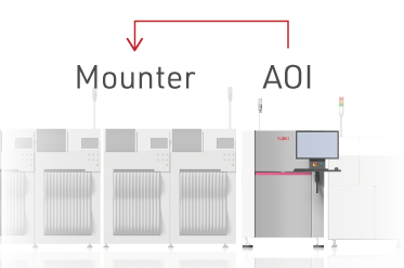
M2M Co-Operation with Pick-and-Place Machine
Saki AOI machines are developed for M2M communication with all major surface mount machine manufacturers.
The AOI provides feedback to the surface mount machine regarding the mounting position, greatly strengthening quality assurance.
Saki’s Total Lineup Solution
Saki’s 3D-AOI uses a common platform with 3D-SPI and 3D-CT-AXI.
The process is consistent throughout – from post-printing solder inspection using SPI, through to the inspection of mounted components.
Insertion Inspection Solution
Saki provides a wide range of inspection solutions suitable for tall inserted components, such as character and polarity inspection of tall parts, and simultaneous measurement of the solder on the board and the height of tall parts. (With Z-axis option)
Back-Side Solder Inspection Solution
The 3D-AOI automates solder inspection, supporting flow, dip, and selective soldering.
Automation guarantees a more consistent quality than visual inspection, improving the solder inspection process and saving on labor.
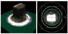
THT solder inspection algorithm
Using 3D information, one algorithm covers all the necessary inspection items such as pin height, solder fillet height, and bridge inspection.
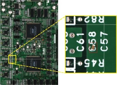
Extra Component Detection (ECD) doesn’t miss any fallen objects or surplus parts
By generating statistical sample data from approximately ten defect-free images, defects such as unexpected surplus parts, solder balls, and dust in the board can be automatically detected. Even without prepared samples, defects such as solder balls can be detected using design data and threshold information.
ECD NG Images
Specifications
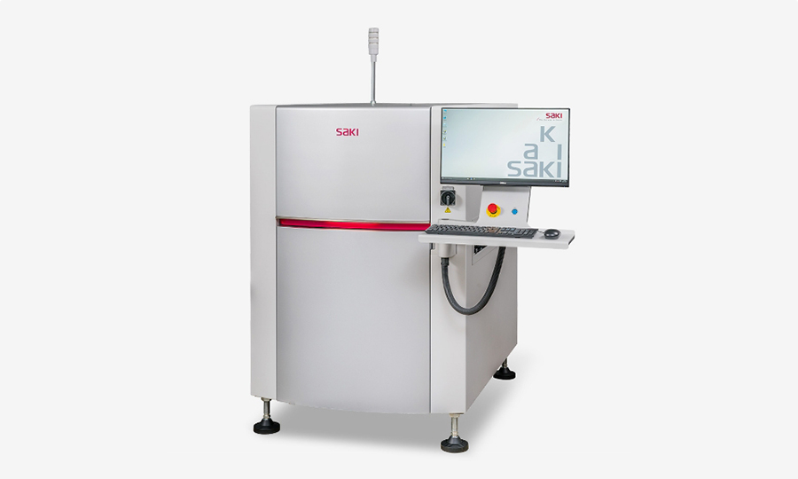
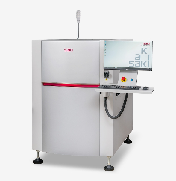
3Di-LS3EX (L size・Arm type)
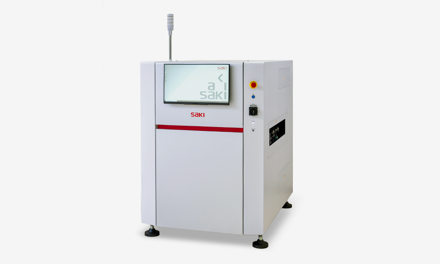
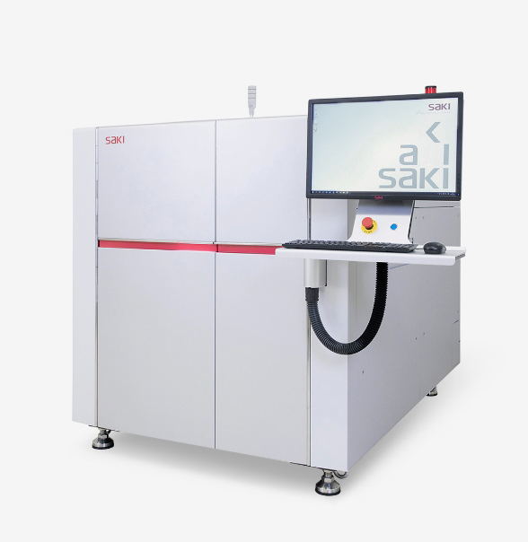
3Di-LS3EX (L size・Built-in type)
Specifications
| Dimensions | M | L | XL |
|---|---|---|---|
| Model | 3Di-MS3EX | 3Di-LS3EX | 3Di-ZS3EX |
| Size[Main body] (W) x (D) x (H) mm (in.) | 850×1480×1500 (33.46 x 58.27 x 59.06) | 1040×1480×1500 (40.94 x 58.27 x 59.06) | 1840×1480×1520 (72.44 x 58.27 x 59.84) |
| Resolution | 8μm、15μm | 8μm、15μm | 15μm*1 |
| PCB Clearance mm (in.) | Top: 40 (1.57) Bottom: 60 (2.36) *2 | ||
| Electric Power Requirement | Single-phase ~ 200-240V+/-10%, 50/60Hz | ||
| PCB Size (W)×(L)mm (in.) | 50 x 60 – 330 x 330 (1.97 x 2.36 – 12.99 x 12.99 ) | 50 x 60 – 510 x 510 (1.97 x 2.36 – 20.07 x 20.07)*3 | 50 x 60 – 686 x 1016 (1.97 x 2.36 – 27.00 x 40.00)*4 |
| Weight | 850kg | 900kg | 980kg |
| Dimensions | M |
|---|---|
| Model | 3Di-MS3EX |
| Size[Main body] (W) x (D) x (H) mm (in.) | 850×1430×1500 (33.46 x 56.30 x 59.06) |
| Resolution | 8μm、15μm |
| PCB Clearance mm (in.) | Top: 40 (1.57) Bottom: 60 (2.36)*2 |
| Electric Power Requirement | Single-phase ~ 200-240V+/-10%, 50/60Hz |
| PCB Size (W)×(L)mm (in.) | 50 x 60 – 330 x 330 (1.97 x 2.36 – 12.99 x 12.99 ) |
| Weight | 850kg |
| Dimensions | L |
|---|---|
| Model | 3Di-LS3EX |
| Size[Main body] (W) x (D) x (H) mm (in.) | 1040×1480×1500 (40.94 x 58.27 x 59.06) |
| Resolution | 8μm、15μm |
| PCB Clearance mm (in.) | Top: 40 (1.57) Bottom: 60 (2.36)*2 |
| Electric Power Requirement | Single-phase ~ 200-240V+/-10%, 50/60Hz |
| PCB Size (W)×(L)mm (in.) | 50 x 60 – 510 x 510 (1.97 x 2.36 – 20.07 x 20.07)*3 |
| Weight | 900kg |
| Dimensions | XL |
|---|---|
| Model | 3Di-ZS3EX |
| Size[Main body] (W) x (D) x (H) mm (in.) | 1840×1480×1520 (72.44 x 58.27 x 59.84) |
| Resolution | 15μm*1 |
| PCB Clearance mm (in.) | Top: 40 (1.57) Bottom: 60 (2.36)*2 |
| Electric Power Requirement | Single-phase ~ 200-240V+/-10%, 50/60Hz |
| PCB Size (W)×(L)mm (in.) | 50 x 60 – 686 x 1016 (1.97 x 2.36 – 27.00 x 40.00)*4 |
| Weight | 980kg |
*1 Imaging speed when equipped with a Z axis. The XL size comes standard with a Z axis.
*2 For dual mode, the PCB Clearance Bottom is 50mm (1.96 in.),
*3 For dual mode, the PCB Size is 50×60〜320×510 (1.97 x 2.36 – 12.60 x 20.07)
*4 An expansion to 60 inches (686 x 1524) is optional.
Use Case
Alps Alpine Co., Ltd.
Alps Alpine Co., Ltd., a global company operating a business centered on electronic components and automotive information systems, has installed Saki’s SPI and AOI.
Marquardt
Marquardt, a leading German manufacturer of mechatronic products for the automotive industry, has installed Saki’s 3D-AOI and 3D-CT-AXI solutions.
TQ-Group
TQ-Group, a major German electronics solution provider, has installed Saki’s 3D-AOI and 3D-SPI solutions.

Rohde & Schwarz
Rohde & Schwarz, a major German electronics solution provider, has installed Saki’s 3D-AOI and 3D-SPI solutions.
Smart Modular Technologies
Smart Modular Technologies, manufacturer of high-performance DRAM modules and solid-state disk drives (SSDs), has installed Saki’s 3D-AOI and 3D-SPI solutions.
Related Solutions
3D-SPI
3D Solder Paste
Inspection Machine
3D-CT AXI
Inline 3D-CT Automated
X-ray Inspection Systems
2D-AOI
2D Automated Optical Inspection Systems