Inline 3D-CT Automated X-ray Inspection Systems for XXL PCBs
Next-
Generation
AXI
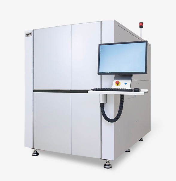
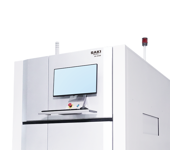
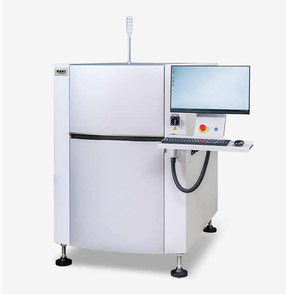
3Xi-ZS1EX is a next-generation automated X-ray inspection (AXI) system designed for large-format (XXL) PCB applications. Combining a compact footprint with high-resolution 3D CT imaging and advanced AI-assisted inspection, it supports stable, high-throughput inspection of complex assemblies used in data center and AI infrastructure applications.
Key Features
- Inspect all PCB sizes up to XXL formats with a compact footprint
- High-speed, high-resolution 3D CT imaging
- Designed for tall components such as press-fit pins
- Built-in AI-assisted image analysis for enhanced inspection performance
01

Reliable High-Precision Inspection for Large Format PCBs
- Accurate Defect Detection with High-Resolution 3D Imaging
- Proprietary “Planar CT” Technology
- AI-Powered Inspection for Better Quality and Efficiency

Accurate Defect Detection with High-Resolution 3D Imaging
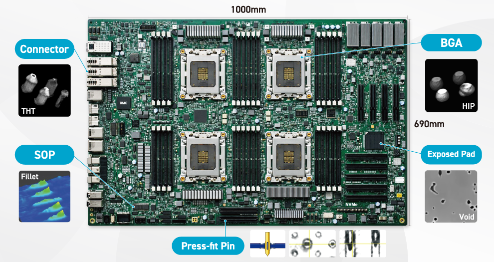
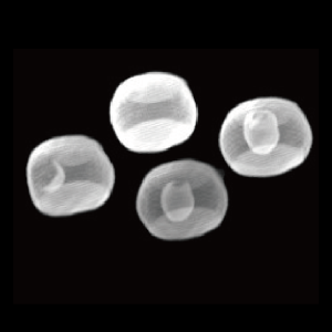
Advanced 3D CT technology enables highly accurate detection of defects such as BGA voids and non-wetting.
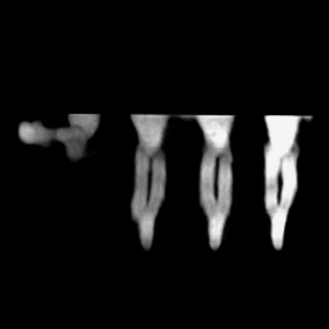
Press-fit components commonly used in large server PCBs are captured clearly in 3D, ensuring reliable detection of bent or missing pins.
Example of Defect Detection Using High-Definition Image Aquisition
Head in Pillow
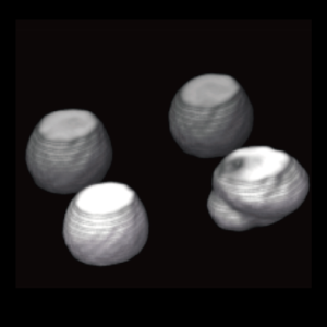
Void Defect
Press-fit Defect
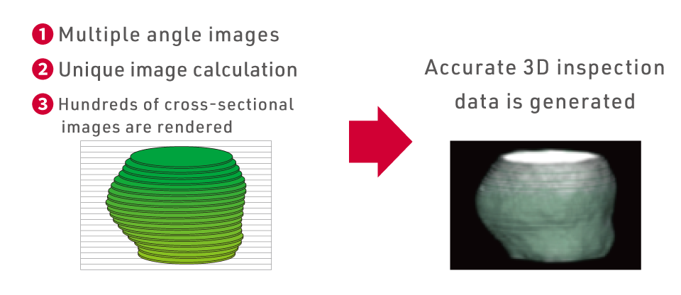
Proprietary “Planar CT” Technology
SAKI’s unique planar CT technology rapidly captures hundreds of high-resolution tomographic images.
These are reconstructed into highly accurate 3D data, providing clear visualization of complex structures and even microscopic defects.
High-precision Correction Technology
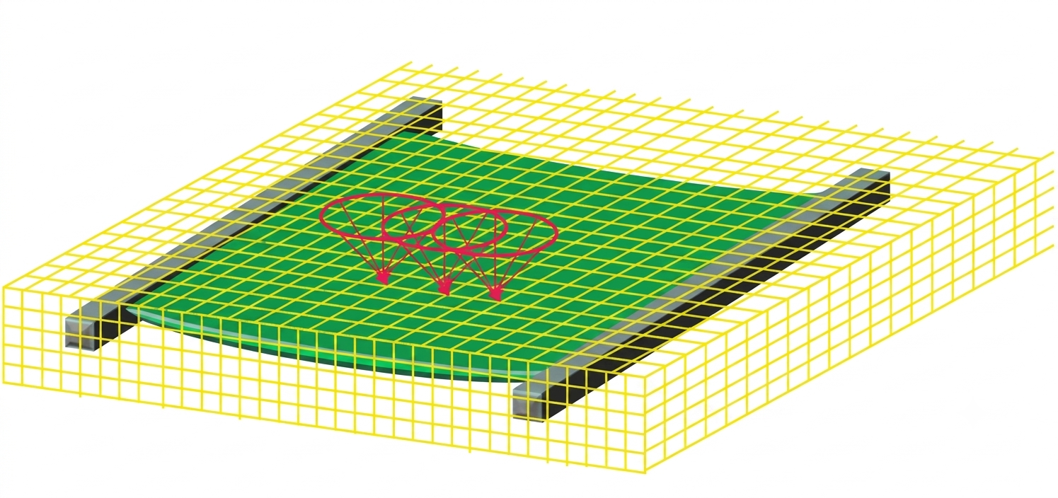
Generating high-definition 3D imagery requires high-precision correction technology. SAKI’s 3D-AXI utilizes pattern data, an automatic board warp correction function in the XYZ directions, and a positioning function to help improve inspection accuracy while simplifying inspection program creation.
One Piece Function
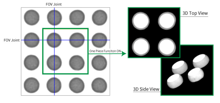
Even with large format PCBs, where warpage can significantly impact results, the system automatically identifies reference patterns and performs precise corrections.
This helps maintain stable and repeatable inspection performance even on warped large-format PCBs.
AI-Powered Inspection for Better Quality and Efficiency
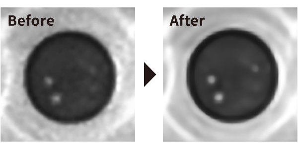
AI Denoise
AI-driven noise reduction enhances image clarity, helping improve the detection of small voids and other subtle defects and dramatically improving inspection performance.
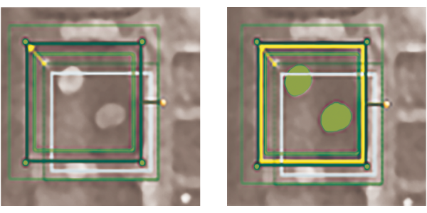
AI Inspect Void
Eliminates the need for manual parameter adjustment in void detection.
The algorithm automatically applies optimized inspection conditions to help maintain consistent inspection performance despite variations in imaging conditions.
02

Hardware Designed for High Productivity
- Compact Design with Large Board Capability
- Robust Hardware Architecture
- Flexible Clearance for Complex Assemblies
Compact Design with Large Board Capability
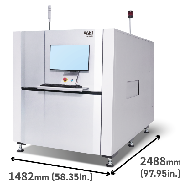
Despite its compact footprint, the system supports PCB sizes up to 1000 x 690 mm (XXL).
It is ideal for space-constrained production environments and capable of handling today’s increasingly large and complex server boards.
Increased Throughput with High Inspection Performance
Compared to previous models, takt time is improved by approximately 1.6 times.
The optimized system design delivers faster inspection while maintaining high accuracy, helping improve throughput in high-volume production environments.
Robust Hardware Architecture
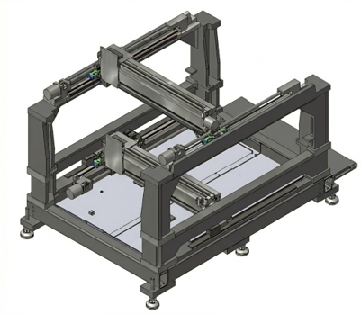
SAKI’s proprietary hardware design achieves both speed and precision:
・High-rigidity frame construction for durability and repeatability
・Dual-axis gantry system for stable motion
・Fully enclosed motor drive for precise positioning at high speeds
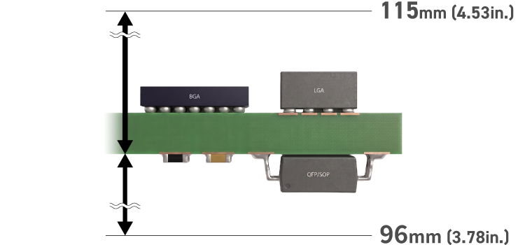
Flexible Clearance for Complex Assemblies
Designed with ample clearance to accommodate double-sided PCBs and tall components.
This flexibility supports the inspection of diverse board designs and assembly configurations.
Airless Design for Faster Startup Time
The airless shutter system enables faster operation and eliminates the need for air adjustments.
Benefits include:
・Reduced startup time
・Improved takt time
・Lower energy consumption and reduced CO₂ emissions
03

User-Friendly Operation and Maintenance
- Easy programming
- Debugging Without Stopping the Production Line
- X-ray dosage simulator
Easy Programming
Inspection program creation is significantly simplified:
・Use of design data
・Automatic imaging condition settings per FOV
This reduces setup time and improves operational efficiency.
Debugging Without Stopping the Production Line
The offline debugging function enables the collection and debugging of images without the need to stop the machine operations. Alongside real-time library updates, a catalogue of historic defect data is saved and can be re-inspected, supporting continuous process improvement and quality assurance.
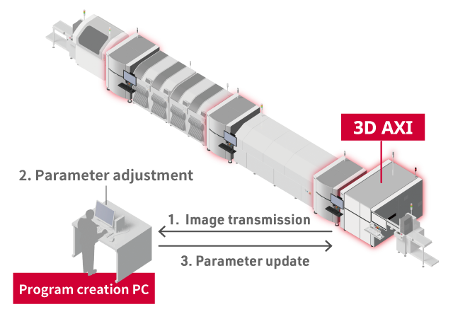
Advantages of cooperation with AOI
For ease of operability, SAKI’s 3D-AXI inspection machine runs on the same software platform as its AOI solutions. By ensuring consistent quality control across the production line, inspection results from both AOI and AXI are integrated and displayed on the same screen.
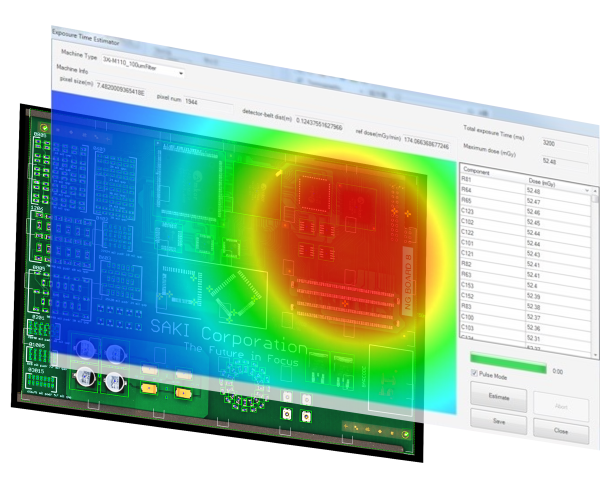
X-ray Dosage Simulator
When performing X-ray inspections, managing radiation exposure is an important consideration for electronic assemblies. SAKI’s X-ray inspection equipment is equipped with an exposure dose simulator, predicting the exposure dose for each area to optimize imaging conditions. X-rays are generated only during image acquisition, minimizing exposure.
X-ray Dosage Simulator
Optimal Functions for Each Process
SMT
- Example of SMT Process Defect Detection
Backend
- Example of defect detection in backend process
- SAKI’s total lineup solution
Examples of SMT Process Defect Detection
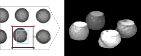
BGA Head in Pillow
The 3D-AXI clearly separates unwetted shapes traditionally difficult to detect, performing inspection using the volume ratio and shape of solder balls.
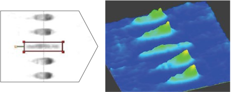
BGA Void Defect
The automatic inspection of both void volume ratio and void area ratio ensures that no voids, no matter how small, are overlooked.
IC Components Solder Defect
Pass / fail judgments are based on changes in fillet position, height, width, angle, and number of IC components. If solder crosses between leads, it is detected as a bridge defect.
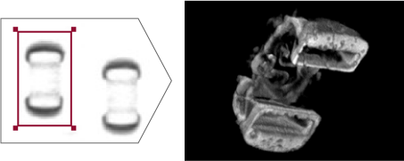
Chip Components Solder Defect
Pass / fail judgments are based on changes in fillet position, height, width, angle, and number of chip parts.
Examples of Defect Detection in Backend Process
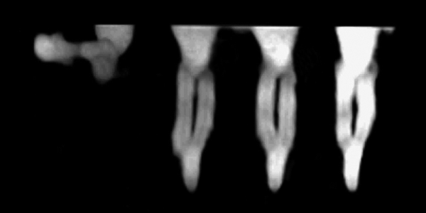
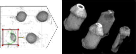
Insertion Part: Press-fit Components Insertion Defect
If the pin is not inserted to the specified depth of the through-hole, it is detected as an insertion defect (NG).
Insertion Part: Insufficient Solder Filling
The 3D-AXI measures the solder filling rate inside the through-hole and reliably detects defects that are missed by general tomographic image area inspection.
All inspections meet, or exceed, IPC standards.
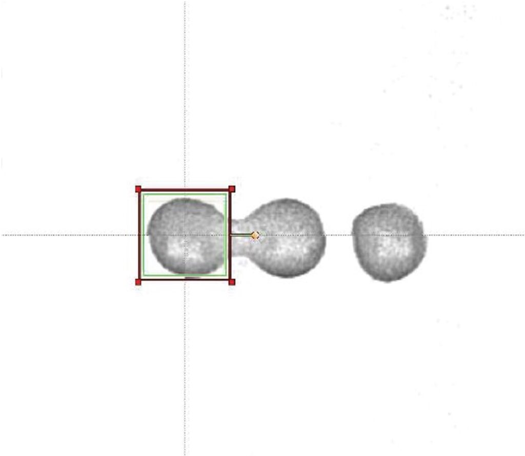
Insertion Part: Faulty Bridge
If solder crosses between the leads, it is detected as a bridge defect.
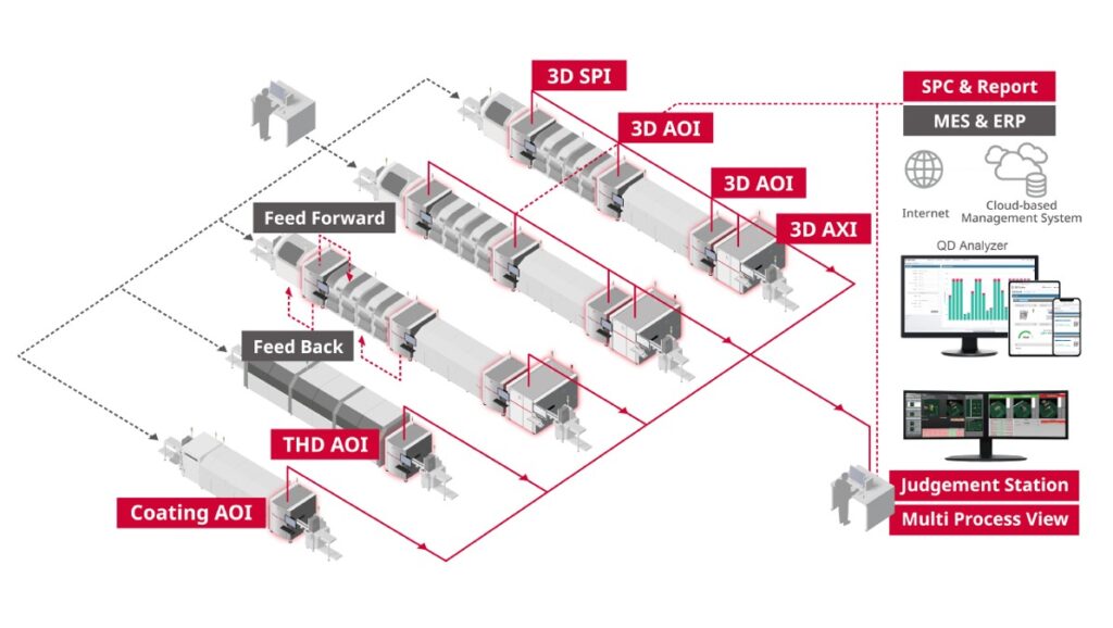
SAKI’s Total Line Solutions
SAKI’s 3D AOI uses a common platform with 3D SPI and 3D CT AXI.
We can cover everything from post-printing solder inspection using SPI to inspection of mounted components with a consistent operation.
Specification
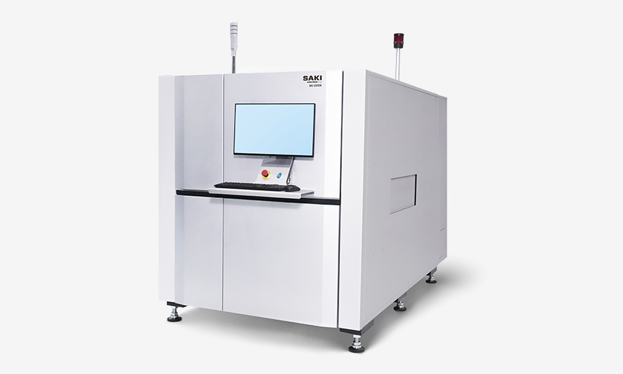
3Xi-ZS1EX
| Model | 3Xi-ZS1EX |
|---|---|
| X-ray Tube | 130 kV 39 W Closed X-ray Source |
| Size (W)×(D)×(H)mm (in.) | 1,482 x 2,488 x 1,630 (58.35 x 97.95 x 64.17) |
| Resolution | 5 – 27μm*1 |
| PCB Clearance | Top: 115 – 130mm (4.53 – 5.12 in.) / Bottom: 96mm(3.78 in.)*2 |
| Electric Power Requirement | Three Phase 200-240V ±5 %、50/60 Hz 3.1 kVA |
| X-ray Leakage | 1.0 μSv/h or less |
| PCB Size (L)×(W)mm (in.) | 120 x 50 – 1,000 x 690 ( 4.73 x 1.97 – 39.37 x 27.17 ) |
| Weight | Aprox. 3,500 kg |
*1 Resolution varies depending on customer specifications.
*2 The maximum top-side component height may vary depending on customer specifications and board warpage.
Related Solutions
3D-SPI
3D Solder Paste
Inspection Machine
3D-AOI
3D Automated Optical Inspection Systems
Power Module-AXI
Inline 3D X-ray Inspection Machine for IGBT Power Modules